

Philips 74f378 DATASHEETS

INTEGRATED CIRCUITS
74F378
Hex D flip-flop with enable
Product specification
IC15 Data Handbook
1989 Oct 05

Philips Semiconductors Product specification
74F378Hex D flip-flop with enable
FEA TURES
•6-bit high-speed parallel register
•Positive edge-triggered D-type inputs
•Fully buffered common Clock and Enable inputs
•Input clamp diodes limit high speed termination effects
•Fully TTL and CMOS compatible
DESCRIPTION
The 74F378 has six edge-triggered D-type flip-flops with individual
D inputs and Q outputs. The common buffered Clock (CP) input
loads all flip-flops simultaneously when the Enable (E
The register is fully edge-triggered. The state of each D input, one
setup time before the Low-to-High clock transition is transformed to
the corresponding flop-flop’s Q output. The E
one setup time prior to the Low-to-High clock transition for
predictable operation.
PIN CONFIGURATION
16
V
CC
15
Q5
14
D5
13
D4
12
Q4
11
D3
107
Q3
98
CP
GND
Q0
D0
D1
Q1
D2
Q2
1
E
2
3
4
5
6
) input is Low.
input must be stable
TYPE TYPICAL f
max
TYPICAL SUPPL Y
CURRENT (TOTAL)
74F378 100MHz 35mA
ORDERING INFORMATION
COMMERCIAL
DESCRIPTION
16–pin plastic DIP N74F378N SOT38-4
16–pin plastic SO N74F378D SOT109-1
RANGE
= 5V ±10%,
V
CC
T
= 0°C to +70°C
amb
PKG DWG #
SF00927
INPUT AND OUTPUT LOADING AND FAN OUT TABLE
PINS DESCRIPTION 74F (U.L.)
HIGH/LOW
D0 – D5 Data inputs 1.0/1.0 20µA/0.6mA
CP Clock pulse input (active rising edge) 1.0/1.0 20µA/0.6mA
E Enable input (active low) 1.0/1.0 20µA/0.6mA
Q0 – Q5 Data outputs 50/33 1.0mA/20mA
NOTE:
One (1.0) FAST unit load is defined as: 20µA in the High state and 0.6mA in the Low state.
LOAD VALUE
HIGH/LOW
1989 Oct 05 853–0067 97804
2
Philips Semiconductors Product specification
74F378Hex D flip-flop with enable
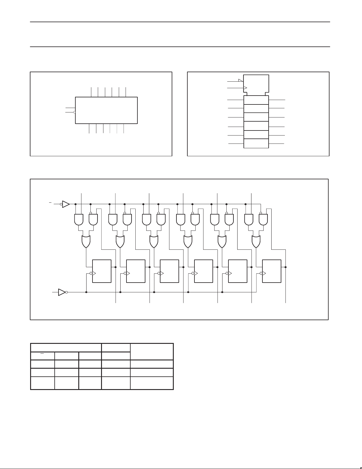
LOGIC SYMBOL
9
1
V
= Pin 16
CC
GND = Pin 8
LOGIC DIAGRAM
1
E
34 6111314
D0 D1 D2 D3 D4 D5
CP
E
Q0 Q1 Q2 Q3 Q4 Q5
2 5 7 101215
D0
3
D1
SF00916
4
IEC/IEEE SYMBOL
1
G1
9
3
4
6
11
13
14
D2
6
D3
11
D4
13
1C2
2D
D5
14
2
5
7
10
12
15
SF00917
9
CP
V
= Pin 16
CC
GND = Pin 8
DQ
CP
DQ
CP
2
Q0
FUNCTION TABLE
INPUTS OUTPUTS
E CP Dn Qn
l ↑ h H Load “1”
l ↑ l L Load “0”
h
H
H = High-voltage level
h = High-voltage level one setup time
prior to the Low-to-High clock transition
L = Low-voltage level
l = Low-voltage level one setup time
prior to the Low-to-High clock transition
X = Don’t care
↑ = Low-to-High clock transition
↑
X
X
X
no change
no change
DQ
5
Q1
OPERATING
MODE
Hold (do nothing)
CP
7
Q2
DQ
CP
Q3
DQ
10
CP
Q4
12
DQ
CP
15
Q5
SF00918
1989 Oct 05
3
 Loading...