

Philips 74f350 DATASHEETS
Philips Semiconductors FAST Products Product specification
74F3504-bit shifter
1
March 20, 1989 853–0368 96093
FEATURES
•Shifts 4 bits of data to 0, 1, 2, 3 places under control of two
select lines
•3-State outputs for bus organized systems
DESCRIPTION
The 74F350 is a combination logic circuit that shifts a 4-bit word
from 0 to 3 places. No clocking is required as with shift registers.
The 74F350 can be used to shift any number of bits any number of
places up or down by suitable interconnection. Shifting can be:
1. Logical — with logic zeros filled in at either end of the shifting
field.
2. Arithmetic — where the sign bit is extended during a shift down.
3. End around — where the data word forms a continuous loop.
The 3-State outputs are useful for bus interface applications or
expansion to a larger number of shift positions in end around
shifting. The active Low Output Enable (OE
) controls the state of the
outputs. The outputs are in the high impedance “off” state when OE
is High, and they are active when OE is Low.
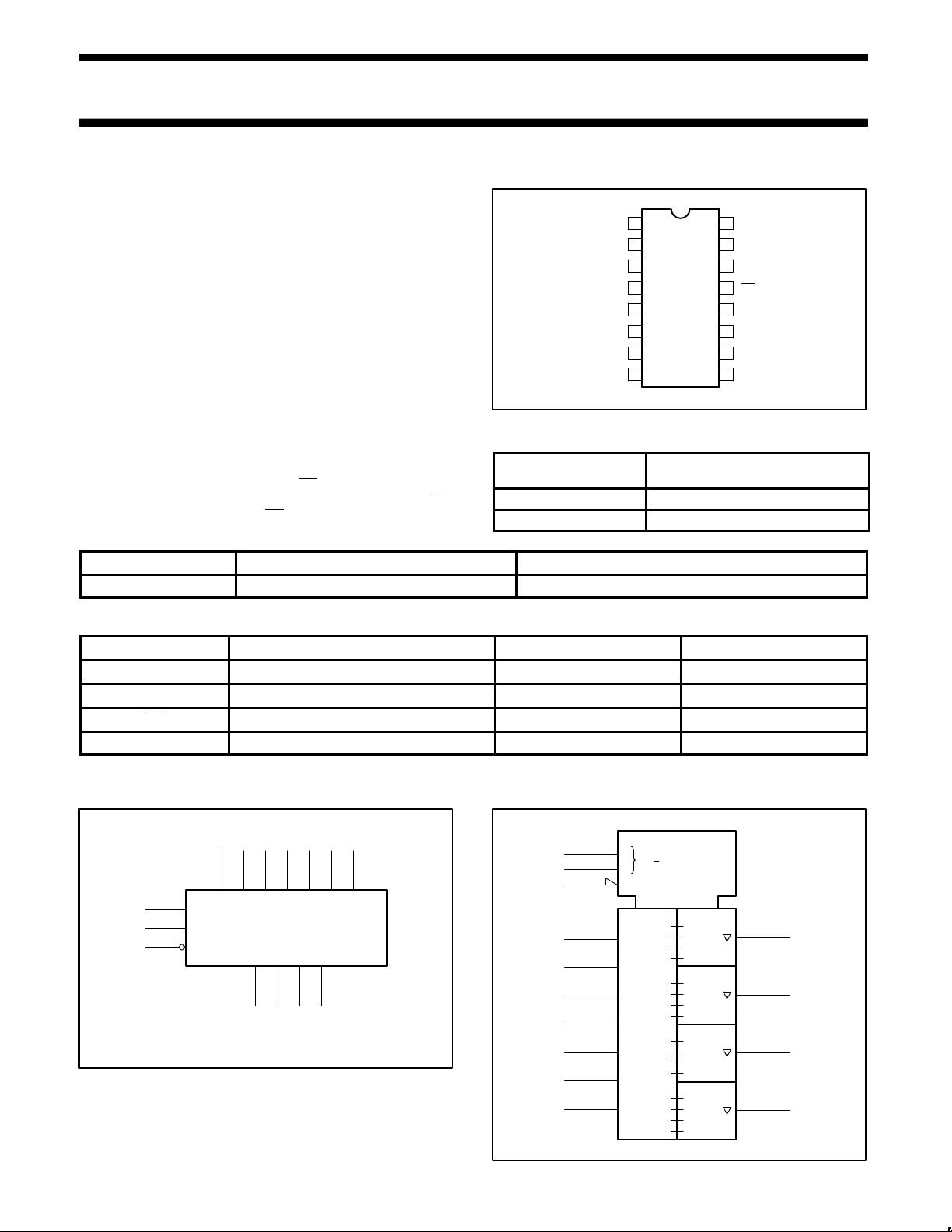
PIN CONFIGURATION
16
15
14
13
12
11
107
6
5
4
3
2
1
I3
V
CC
Y2
Y3
S0
OE
Y0
Y1
I–3
I–2
I2
I–1
I0
I1
98GND S1
SF00205
ORDERING INFORMA TION
DESCRIPTION
COMMERCIAL RANGE
V
CC
= 5V ±10%, T
amb
= 0°C to +70°C
16-pin plastic DIP N74F350N
16-pin plastic SO N74F350D
TYPE TYPICAL PROPAGATION DELAY TYPICAL SUPPLY CURRENT (TOTAL)
74F350 5.2ns 24mA
INPUT AND OUTPUT LOADING AND FAN-OUT TABLE
PINS DESCRIPTION 74F (U.L.) HIGH/LOW LOAD VALUE HIGH/LOW
I–n, In Data inputs 1.0/2.0 20µA/1.2mA
S0, S1 Select inputs (active Low) 1.0/2.0 20µA/1.2mA
OE Output Enable input (active Low) 1.0/2.0 20µA/1.2mA
Y0 – Y3 Data outputs 150/40 3.0mA/24mA
NOTE: One (1.0) FAST unit load is defined as: 20µA in the High state and 0.6mA in the Low state.
LOGIC SYMBOL
VCC = Pin 16
GND = Pin 8
SF00206
9
10
13
S1
S0
OE
1 2 3 4 5 6 7
I–3 I–2 I–1 I0 I1 I2 I3
Y0 Y1 Y2 Y3
15 14 12 11
IEC/IEEE SYMBOL
SF00207
0
9
10
D MUX
13
G
0
3
[
SHIFTER
]
1
EN
≥1
15
10 3
11 2
12 1
13 0
≥1
14
11 3
12 2
13 1
14 0
≥1
12
12 3
13 2
14 1
15 0
≥1
11
13 3
14 2
15 1
16 0
Z10
1
Z11
2
Z12
3
Z13
4
Z14
5
Z15
6
Z16
7
Philips Semiconductors FAST Products Product specification
74F3504-bit shifter
March 20, 1989
2
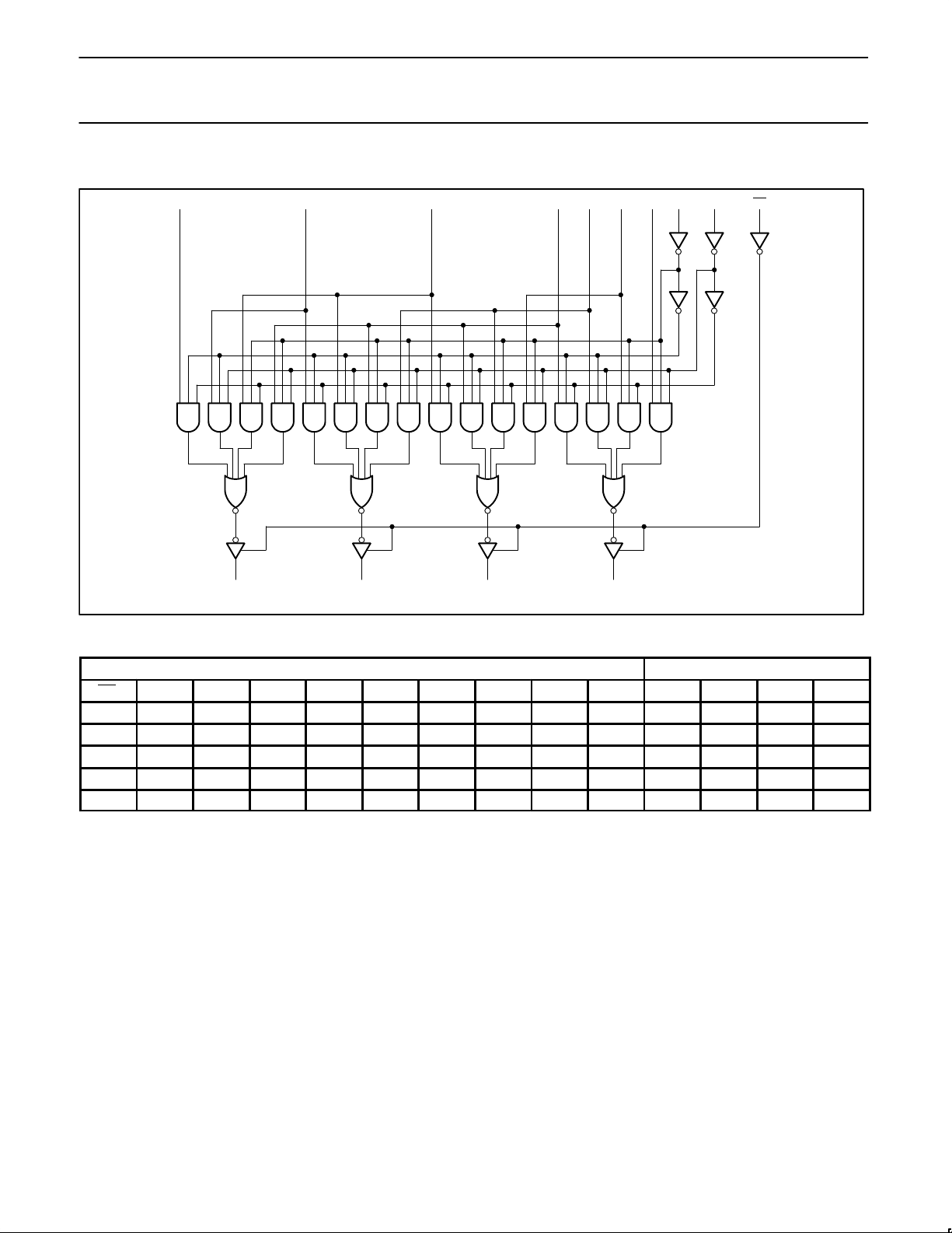
LOGIC DIAGRAM
139 10
V
CC
= Pin 16
GND = Pin 8
OE
S1 S0
SF00208
1
I–3
Y0
15
2
I–2
Y1
14
3
I–1
Y2
12
4
I0
Y3
11
5I16I27
I3
OUTPUTS
OE S1 S0 I3 I2 I1 I0 I–1 I–2 I–3 Y3 Y2 Y1 Y0
H X X X X X X X X X Z Z Z Z
L L L D3 D2 D1 D0 X X X D3 D2 D1 D0
L L H X D2 D1 D0 D–1 X X D2 D1 D0 D–1
L H L X X D1 D0 D–1 D–2 X D1 D0 D–1 D–2
L H H X X X D0 D–1 D–2 D–3 D0 D–1 D–2 D–3
H = High voltage level
L = Low voltage level
X = Don’t care
Z = High impedance “off” state
Dn = High or Low state of referenced In input
FUNCTION TABLE
INPUTS
 Loading...