

Philips 74f323 DATASHEETS
Philips Semiconductors
Product specification
74F323
8-bit universal shift/storage register with synchronous
reset and common I/O pins (3-State)
1
1990 Mar 01 853-0367 98987
FEATURES
•Common parallel I/O for reduced pin count
•Additional serial inputs and outputs for expansion
•Four operating modes: Shift left, shift right, load, and store
•3-State outputs for bus-oriented applications
DESCRIPTION
The 74F323 is an 8-bit universal shift/storage register with 3-State
outputs. Its function is similar to the 74F299 with the exception of
synchronous Reset. Parallel load inputs and flip-flop outputs are
multiplexed to minimize pin counts. Separate serial inputs and
outputs are provided for flip-flops Q0 and Q7 to allow easy serial
cascading. Four modes of operation are possible: Hold (store), shift
left, shift right, and parallel load.
The 74F323 contains eight edge-triggered D-type flip-flops and the
interstage logic necessary to perform synchronous reset, shift left,
shift right, parallel load, and hold operations. The type of operation is
determined by S0 and S1, as shown in the Function Table. All
flip-flop outputs are brought out through 3-State buffers to separate
I/O pins that also serve as data inputs in the parallel load mode.
Q0 and Q7 are also brought out on other pins for expansion in serial
shifting of longer words.
A Low signal on SR
overrides the Select and inputs and allows the
flip-flops to be reset by the next rising edge of clock. All other state
changes are initiated by the rising edge of the clock. Inputs can
change when the clock is in either state provided only that the
recommended setup and hold times, relative to the rising edge of
clock are observed.
A High signal on either OE
0 or OE1 disables the 3-State buffers and
puts the I/O pins in the high impedance state. In this condition the
shift, hold, load and reset operations can still occur. The 3-State
buffers are also disabled by High signals on both S0 and S1 in
preparation for a parallel load operation.
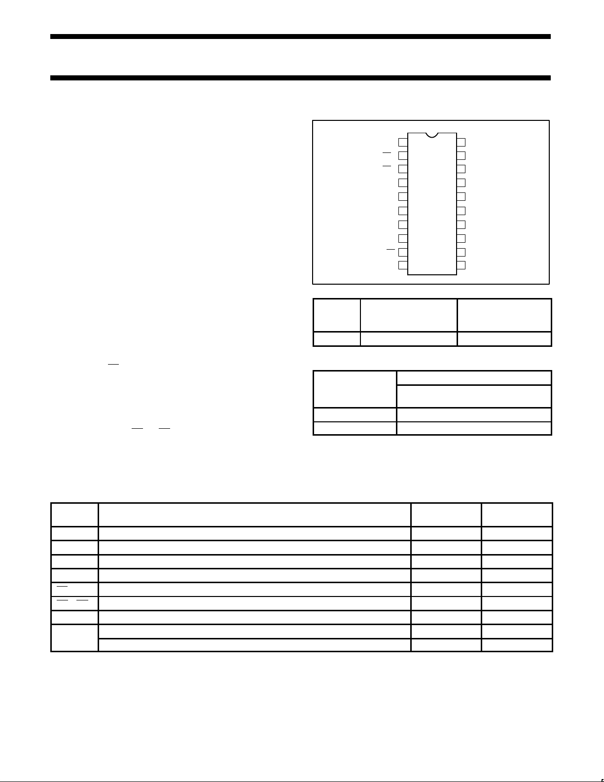
PIN CONFIGURATION
20
19
18
17
16
15
14
13
12
10 11
9
8
7
6
5
4
3
2
1
V
CC
S1
DS7
Q7
I/O7
I/O5
I/O3
I/O1
DS0
S0
I/O6
I/O4
I/O2
I/O0
Q0
OE
0
OE
1
SR
GND
CP
SF00888
TYPE TYPICAL f
MAX
TYPICAL
SUPPLY CURRENT
(TOTAL)
74F323 115MHz 55mA
ORDERING INFORMATION
ORDER CODE
DESCRIPTION
COMMERCIAL RANGE
VCC = 5V ±10%, T
amb
= 0°C to +70°C
20-pin plastic DIP N74F323N
20-pin plastic SOL N74F323D
INPUT AND OUTPUT LOADING AND FAN-OUT TABLE
PINS DESCRIPTION
74F(U.L.)
HIGH/LOW
LOAD VALUE
HIGH/LOW
DS0 Serial data input for right shift 1.0/1.0 20µA/0.6mA
DS7 Serial data input for left shift 1.0/1.0 20µA/0.6mA
S0, S1 Mode select inputs 1.0/2.0 20µA/1.2mA
CP Clock pulse input (Active rising edge) 1.0/1.0 20µA/0.6mA
SR Synchronous Reset input (Active Low) 1.0/1.0 20µA/0.6mA
OE0, OE1 Output Enable input (Active Low) 1.0/1.0 20µA/0.6mA
Q0, Q7 Serial outputs 50/33 20µA/20mA
Multiplexed parallel data inputs or 3.5/1.0 70µA/0.6mA
I/On
3-State parallel outputs 150/40 3.0mA/24mA
NOTE: One (1.0) FAST Unit Load (U.L.) is defined as: 20µA in the High State and 0.6mA in the Low state.
Philips Semiconductors Product specification
74F323
8-bit universal shift/storage register with synchronous
reset and common I/O pins (3-State)
1990 Mar 01
2
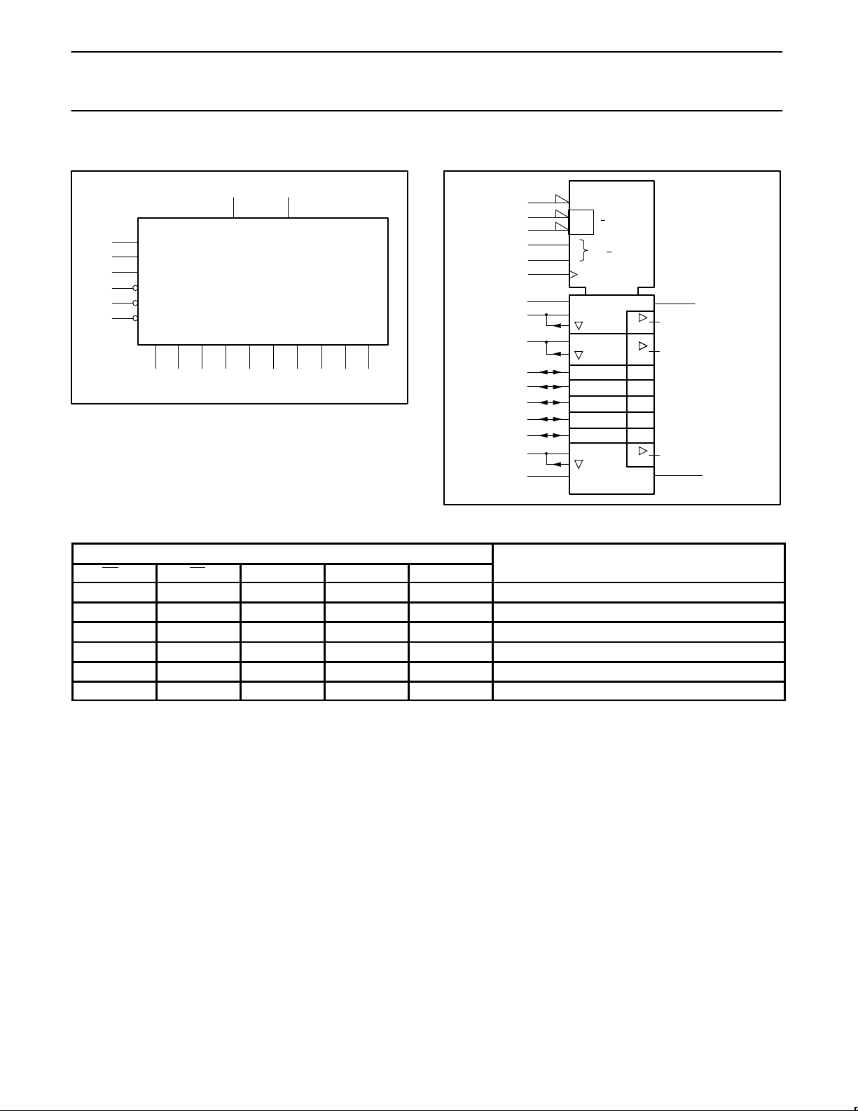
LOGIC SYMBOL
11 18
7 13 6 14 5 15 4 16
1
19
12
9
2
3
Q0 Q7
DS0 DS7
I/O0 I/O2 I/O4 I/O6I/O1 I/O3 I/O5 I/O7
S0
S1
CP
OE0
OE1
SR
V
CC
= Pin 20
GND = Pin 10
8 17
SF00889
LOGIC SYMBOL (IEEE/IEC)
SF00890
&
3
EN13
C4/1→ /2←
9
4R
11
7
6
14
5
15
4
3
12
19
17
8
SRG8
1, 4D
2
1
0
3
M
0
1
3, 4D
5, 13
13
3, 4D
6, 13
3, 4D
12, 13
2, 4D
16
18
Z5
Z6Z6
Z12
FUNCTION TABLE
INPUTS
OEn SR S1 S0 CP
OPERATING MODE
L L X X ↑ Synchronous Reset; Q0 - Q7 = Low
L H H H ↑ Parallel load; I/On → Qn
L H L H ↑ Shift right; DS0 → Q0, Q0 → Q1, etc.
L H H L ↑ Shift left; DS7 → Q7, Q7 → Q6, etc.
L H L L X Hold
H X X X X Outputs disabled (3-state)
H = High voltage level
L = Low voltage level
X = Don’t care
↑ = Low-to-High clock transition
Philips Semiconductors Product specification
74F323
8-bit universal shift/storage register with synchronous
reset and common I/O pins (3-State)
1990 Mar 01
3
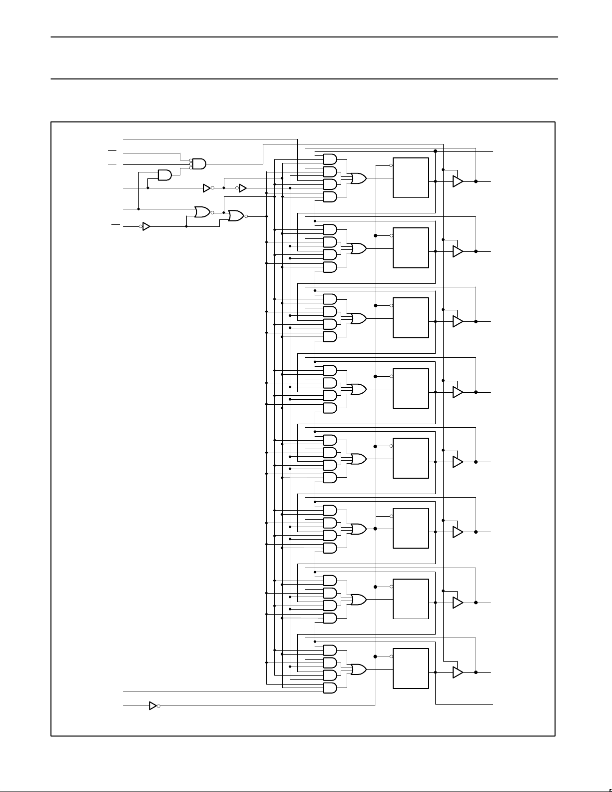
LOGIC DIAGRAM
Q
Q7
I/O7
S0
D
CP
Q
I/O6
D
CP
Q
I/O5
D
CP
Q
I/O4
D
CP
Q
I/O3
D
CP
Q
I/O2
D
CP
Q
I/O1
D
CP
Q
I/O0
D
CP
Q0
CP
DS0
S1
OE1
OE
0
DS7
SF00883
18
2
3
19
1
11
12
VCC = Pin 20
GND = Pin 10
17
16
4
15
5
14
6
13
7
8
SR
9
 Loading...