

Philips 74f298 DATASHEETS
INTEGRATED CIRCUITS
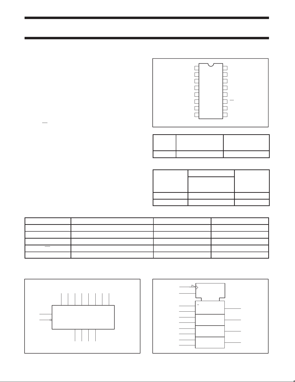
74F298
Quad 2-input multiplexer with storage
Product specification
IC15 Data Handbook
1989 Aug 14
Philips Semiconductors Product specification
74F298Quad 2-input multiplexer with storage
FEA TURES
•Fully synchronous operation
•Select from two data sources
•Buffered, negative edge triggered clock
•Provides the equivalent of function capabilities of two separate
MSI functions (74F157 and 74F175)
DESCRIPTION
The 74F298 is a high speed Quad 2-Input Multiplexer with storage.
It selects 4 bits of data from two sources (ports) under the control of
a common Select input (S). The selected data is transferred to the
4-bit output register synchronous with the High-to-Low transition of
the clock (CP). The 4-bit register is fully edge triggered. The data
inputs (I0 and I1) and Select input (S) must be stable only one setup
time prior to the High-to-Low transition of the clock for predictable
operation.
PIN CONFIGURATION
I1b
1
I1a
2
I0a
3
I0b
4
I1c
5
I1d
6
I0d
TYPE TYPICAL f
MAX
74F298 115MHz 30mA
16
V
CC
Qa
15
Qb
14
Qc
13
Qd
12
CP
11
S
107
98GND I0c
SF00859
TYPICAL
SUPPLY CURRENT
(TOTAL)
ORDERING INFORMATION
ORDER CODE
DESCRIPTION
16-pin plastic DIP N74F298N SOT38-4
16-pin plastic SO N74F298D SOT109-1
COMMERCIAL RANGE
VCC = 5V ±10%,
T
= 0°C to +70°C
amb
PKG DWG #
INPUT AND OUTPUT LOADING AND FAN-OUT TABLE
PINS DESCRIPTION 74F (U.L.) HIGH/LOW LOAD VALUE HIGH/LOW
I0a, I0b, I0c, I0d Data inputs 1.0/1.0 20µA/0.6mA
I1a, I1b, I1c, I1d Data inputs 1.0/1.0 20µA/0.6mA
S Select input 1.0/1.0 20µA/0.6mA
CP Clock input (active falling edge) 1.0/1.0 20µA/0.6mA
Qa, Qb, Qc, Qd Data outputs 50/33 1.0mA/20mA
NOTE:
One (1.0) FAST unit load is defined as: 20µA in the High state and 0.6mA in the Low state.
LOGIC SYMBOL
10
11
VCC = Pin 16
GND = Pin 8
S
CP
3241957
I0a I1a I0b I1b I0c I1c I0d
Qa Qb Qc Qd
15 14 13 12
SF00860
6
I1d
LOGIC SYMBOL (IEEE/IEC)
11
10
3
2
4
1
9
5
7
6
C1
M2
2
, 1D
2, 1D
SF00861
15
14
13
12
1989 Aug 14 853–0061 97377
2
Philips Semiconductors Product specification
OPERATING MODE
Load source “0”
Load source “1”
74F298Quad 2-input multiplexer with storage
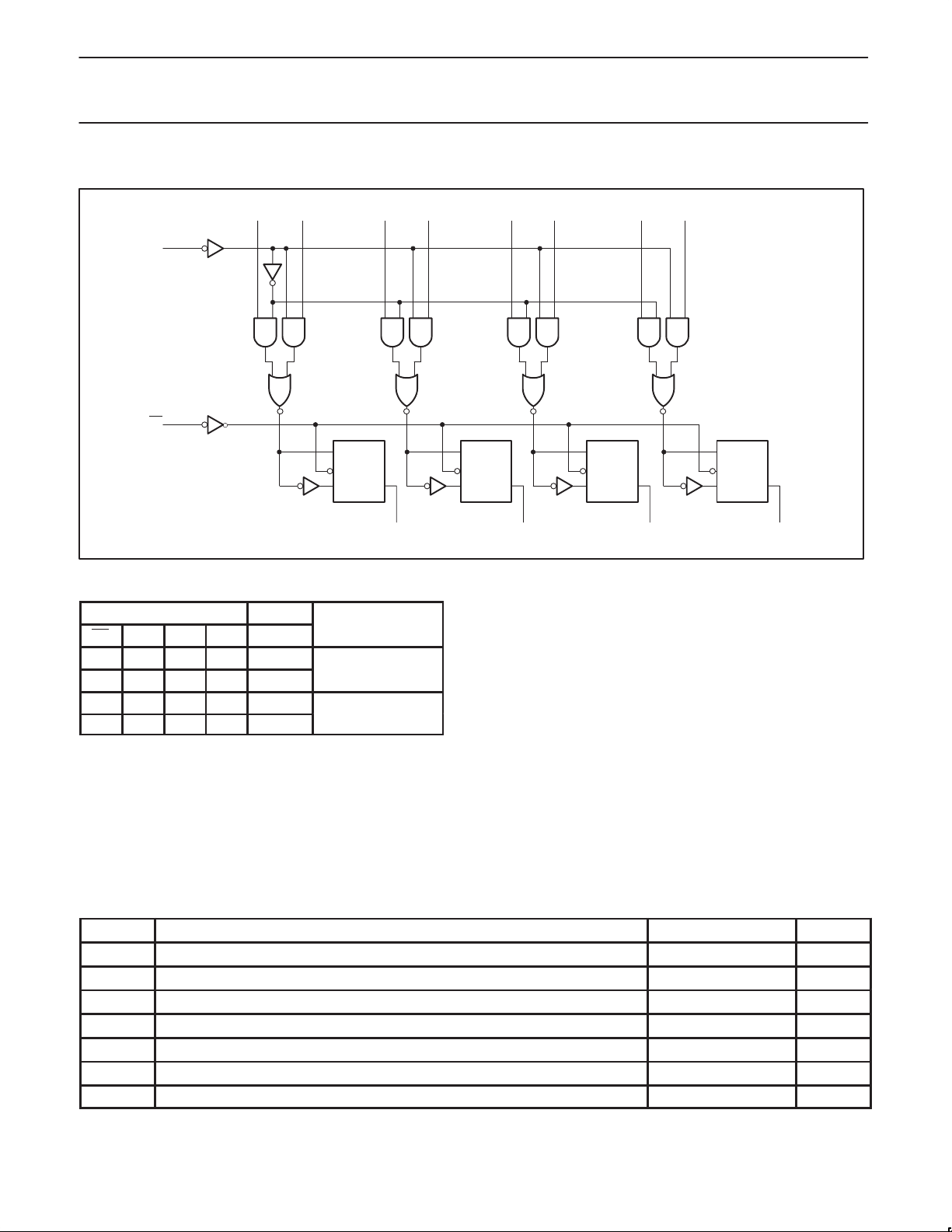
LOGIC DIAGRAM
I1a I0a I1b I0b I1c I0c I1d I0d
23 14 59 67
10
S
11
CP
= Pin 16
V
CC
GND = Pin 8
R
CP
SQa
Qa Qb Qc Qd
15 14 13 12
R
CP
SQb
FUNCTION TABLE
INPUTS OUTPUT
CP S I0n I1n Qn
↓ l l X L
↓ l h X H
↓ h X l L
↓ h X h H
“
”
“
”
H = High voltage level
h = High voltage level one setup time prior to the High-to-Low
clock transition
L = Low voltage level
l = Low voltage level one setup time prior to the High-to-Low
clock transition
X = Don’t care
↓ = High-to-Low clock transition
ABSOLUTE MAXIMUM RATINGS
(Operation beyond the limits set forth in this table may impair the useful life of the device.
Unless otherwise noted these limits are over the operating free-air temperature range.)
SYMBOL
V
CC
V
IN
I
IN
V
OUT
I
OUT
T
amb
T
stg
Supply voltage –0.5 to +7.0 V
Input voltage –0.5 to +7.0 V
Input current –30 to +5 mA
Voltage applied to output in High output state –0.5 to V
Current applied to output in Low output state 40 mA
Operating free-air temperature range 0 to +70 °C
Storage temperature range –65 to +150 °C
PARAMETER RATING UNIT
R
CP
SQc
R
CP
SQd
SF00862
CC
V
1989 Aug 14
3
 Loading...