

Philips 74f2952, 74f2953 DATASHEETS

INTEGRATED CIRCUITS
74F2952
Registered transceiver, non-inverting
(3-State)
74F2953
Registered transceiver, inverting (3-State)
Product specification 1989 Sep 22
IC15 Data Handbook
Philips Semiconductors Product specification
74F2952, 74F2953Transceivers
74F2952 Registered transceiver, non-inverting (3-State)
74F2953 Registered transceiver, inverting (3-State)
FEA TURES
•8-bit registered transceivers
•Two 8-bit, back-to-back registers store data moving in both
directions between two bidirectional buses
•Separate Clock, Clock Enable and 3-State Enable provided for
each register
•74F2952 non-inverting
DESCRIPTION
The 74F2952 and 74F2953 are 8-bit registered transceivers. Two
8-bit back-to-back registers store data flowing in both directions
between two bi-directional buses. Data applied to the inputs is
entered and stored on the rising edge of the Clock (CPXX) provided
that the Clock Enable (CEXX
the 3-State output buffers, but is only accessible when the Output
Enable (OEXX
same as for ‘B’ inputs to ‘A’ outputs.
) is Low. Data flow from ‘A’ inputs to ‘B’ outputs is the
) is Low. The data is then present at
•74F2953 inverting
•AM2952/2953 functional equivalent
•‘A’ outputs sink 24mA and source 3mA
•‘B’ outputs sink 64mA and source 15mA
TYPE
74F2952 160MHz 105mA
74F2953 160MHz 105mA
TYPICAL f
MAX
TYPICAL
SUPPLY CURRENT
(TOTAL)
•300 mil wide 24-pin Slim DIP package
ORDERING INFORMATION
COMMERCIAL RANGE
DESCRIPTION
24-pin Plastic Slim DIP (300mil) N74F2952N, N74F2953N SOT222-1
24-pin Plastic SOL
28-pin Plastic Leaded Chip Carrier N74F2952A, N74F2953A SOT261-2
NOTE:
1. Thermal mounting techniques are recommended. See
mounted devices.
1
SMD Process Applications
VCC = 5V ±10%,
T
= 0°C to +70°C
amb
N74F2952D, N74F2953D SOT137-1
for a discussion of thermal consideration for surface
PACKAGE
DRAWING
NUMBER
INPUT AND OUTPUT LOADING AND FAN-OUT TABLE
PINS DESCRIPTION
A0 – A7 Port A, 3-State inputs 3.5/1.0 70µA/0.6mA
B0 – B7 Port B, 3-State inputs 3.5/1.0 70µA/0.6mA
CPAB, CPBA Clock inputs 1.0/1.0 20µA/0.6mA
CEAB, CEBA Clock Enable inputs 1.0/1.0 20µA/0.6mA
OEAB, OEBA Output Enable inputs 1.0/1.0 20µA/0.6mA
A0 – A7 Port A, 3-State outputs 150/40 3.0mA/24mA
B0 – B7 Port B, 3-State outputs 750/106.7 15mA/64mA
NOTE: One (1.0) FAST unit load is defined as: 20µA in the High state and 0.6mA in the Low state.
74F(U.L.)
HIGH/LOW
LOAD VALUE
HIGH/LOW
1989 Sep 22 853–1097 97708
2
Philips Semiconductors Product specification
74F2952, 74F2953Transceivers
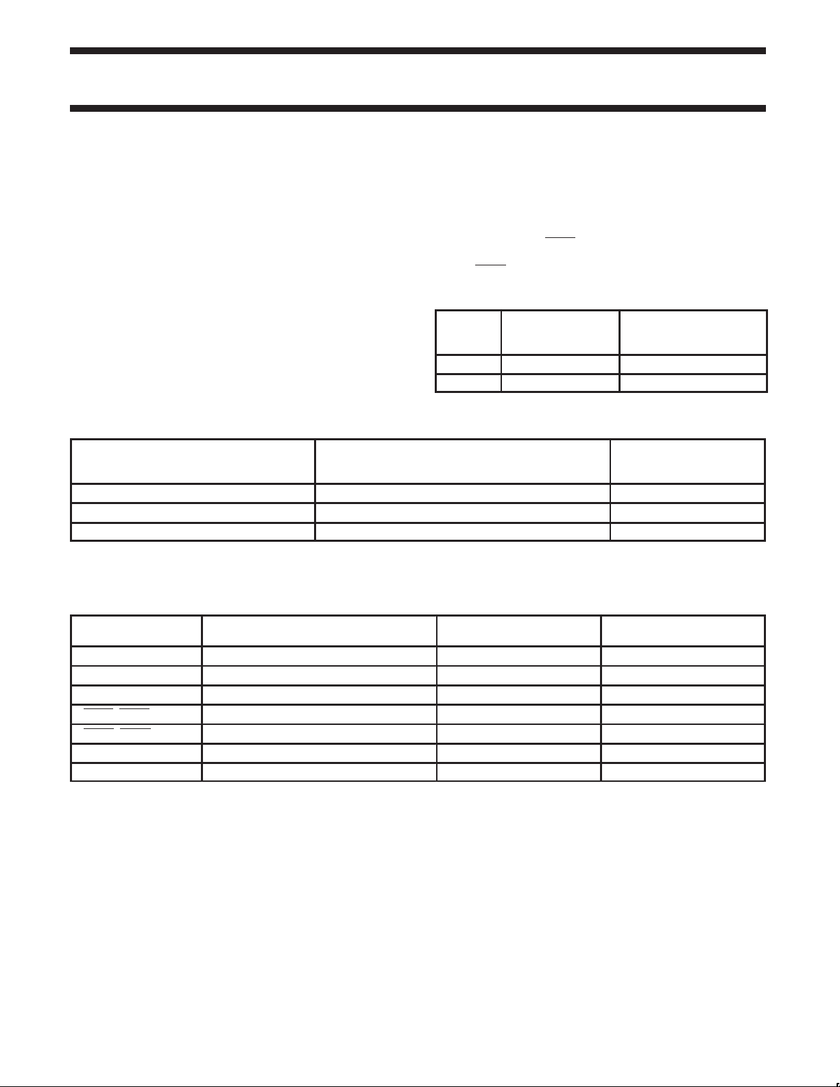
PIN CONFIGURATIONS
DIP – 74F2952
OEAB
CPAB
CEAB
PLCC – 74F2952
5
B4
6
B3
7
B2
8
NC
9
B1
10
B0
11
OEAB
1
B7
2
B6
3
B5
4
B4
5
B3
6
B2
7
B1
8
B0
9
10
11
12 13
GND
B5B6B7NCVccA7A6
1234
12 13 14 15 16 17
NC
GND
CPAB
CEAB
24
23
22
21
20
19
18
17
16
15
14
CEBA
V
CC
A7
A6
A5
A4
A3
A2
A1
A0
OEBA
CPBA
CEBA
SF01371
262728
18
CPBA
25
24
23
22
21
20
19
OEBA
A5
A4
A3
NC
A2
A1
A0
DIP – 74F2953
OEAB
CPAB
CEAB
PLCC – 74F2953
5
4
B
6
B
3
7
B
2
8
NC
9
1
B
10
0
B
11
OEAB
1
7
B
2
B
6
3
B
5
4
4
B
5
B
3
6
B
2
7
1
B
8
B
0
9
10
11
12 13
GND
B5B6B7NCVccA7A6
1234
12 13 14 15 16 17
NC
GND
CPAB
CEAB
24
23
22
21
20
19
18
17
16
15
14
CEBA
V
CC
A7
A
6
5
A
A
4
A
3
2
A
A1
A
0
OEBA
CPBA
CEBA
SF01372
262728
18
CPBA
25
24
23
22
21
20
19
OEBA
A5
A4
A
NC
A
A1
A
3
2
0
1989 Sep 22
SF01373
SF01374
3
Philips Semiconductors Product specification
74F2952, 74F2953Transceivers
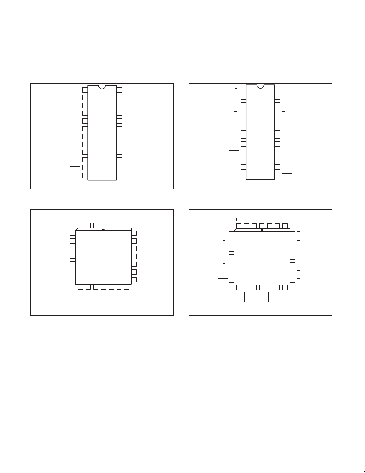
LOGIC SYMBOL – 74F2952
16 17 18 19 20 21 22 23
A0 A1 A2 A3 A4 A5 A6 A7
10
11
14
13
VCC = PIN 24
GND = PIN 12
CPAB
CEAB
CPBA
CEBA
B0 B1 B2 B3 B4 B5 B6 B7
87654321
IEC/IEEE SYMBOL – 74F2952
11
13
15
10
14
16 8
17 7
18 6
19 5
20 4
21 3
22 2
23 1
EN1
EN2
EN3
9
EN4
C5
C6
2,3,6 1,4,5
OEBA
OEAB
SF01375
LOGIC SYMBOL – 74F2953
16 17 18 19 20 21 22 23
A0 A1 A2 A3 A4 A5 A6 A7
10
15
9
11
14
13
VCC = PIN 24
GND = PIN 12
CPAB
CEAB
CPBA
CEBA
B0 B1 B2 B3 B4 B5 B6 B7
87654321
OEBA
OEAB
15
9
SF01376
IEC/IEEE SYMBOL – 74F2953
11
13
15
10
14
16 8
17 7
18 6
19 5
20 4
21 3
22 2
23 1
EN1
EN2
EN3
9
EN4
C5
C6
2,3,6 1,4,5
1989 Sep 22
SF01377
SF01378
4
Philips Semiconductors Product specification
74F2952, 74F2953Transceivers
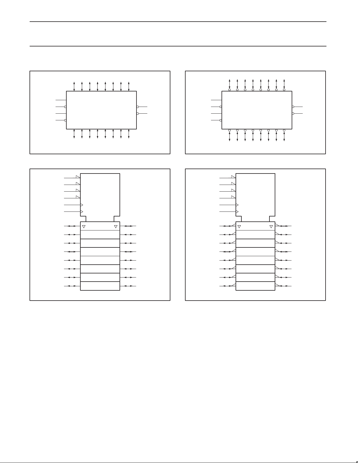
LOGIC DIAGRAM – 74F2952
11
CEAB
10
CPAB
9
OEAB
CE
Q
D
CP
CE
Q
D
CP
CE
Q
D
CP
CE
Q
D
CP
CE
Q
D
CP
CE
Q
D
CP
CE
Q
D
CP
CE
Q
D
CP
CEBA
16
A0
17
A1
18
A2
19
A3
20
A4
21
A5
22
A6
23
A7
13
LOGIC DIAGRAM – 74F2953
11
CEAB
10
CPAB
9
OEAB
CE
16
A0
CE
Q
CP
CE
Q
CP
CE
Q
CP
CE
Q
CP
CE
Q
CP
CE
Q
CP
CE
Q
CP
CE
Q
CP
8
D
D
D
D
D
D
D
D
B0
17
A1
7
B1
18
A2
6
B2
19
A3
5
B3
20
A4
4
B4
21
A5
3
B5
22
A6
2
B6
23
A7
1
B7
CEBA
13
Q
D
CP
CE
Q
CP
CE
Q
D
CP
CE
Q
CP
CE
Q
D
CP
CE
Q
CP
CE
Q
D
CP
CE
Q
CP
CE
Q
D
CP
CE
Q
CP
CE
Q
D
CP
CE
Q
CP
CE
Q
D
CP
CE
Q
CP
CE
Q
D
CP
CE
Q
CP
8
D
D
D
D
D
D
D
D
B0
7
B1
6
B2
5
B3
4
B4
3
B5
2
B6
1
B7
14
CPBA
15
OEBA
V
= PIN 24
CC
GND = PIN 12
1989 Sep 22
SF01379
5
14
CPBA
15
OEBA
V
= PIN 24
CC
GND = PIN 12
SF01380
 Loading...