Philips 74f273a DATASHEETS

INTEGRATED CIRCUITS
74F273A
Octal D flip-flop
Product specification
IC15 Data Handbook
1996 Mar 12

Philips Semiconductors Product specification
74F273AOctal D flip–flop
FEA TURES
• High impedance inputs for reduced loading
µA in Low and High states)
(20
All outputs will be forced Low independently of Clock or Data inputs
by a Low voltage level on the MR
input. The device is useful for
applications where the true output only is required and the CP and
MR
are common to all elements.
• Ideal buffer for MOS microprocessor or memory
• Eight edge–triggered D–type flip–flops
• Buffered common clock
• Buffered asynchronous Master Reset
TYPE
74F273A 170MHz 25mA
TYPICAL
f
MAX
TYPICAL SUPPL Y CURRENT
• See 74F377A for clock enable version
• See 74F373 for transparent latch version
• See 74F374 for 3–State version
DESCRIPTION
The 74F273 has eight edge–triggered D–type flip–flops with
individual D inputs and Q outputs. The common buffered Clock (CP)
and Master Reset (MR
simultaneously .
The register is fully edge–triggered. The state of each D input, one
setup time before the Low–to–High clock transition, is transferred to
the corresponding flip–flop’s Q output.
) inputs load and reset (clear) all flip–flops
ORDERING INFORMATION
COMMERCIAL RANGE
V
PACKAGES
20–pin plastic DIP 74F273AN SOT146-1
20–pin plastic SOL 74F273AD SOT163-1
= 5V±10%;
CC
T
= 0°C to +70°C
amb
INPUT AND OUTPUT LOADING AND FAN-OUT TABLE
PINS DESCRIPTION
D0 – D7 Data inputs 1.0/0.033 20µA/20µA
MR Master Reset input (active–Low) 1.0/0.033 20µA/20µA
CP Clock pulse input (active rising edge) 1.0/0.033 20µA/20µA
Q0 – Q7 Data outputs 50/33 1.0mA/20mA
74F(U.L.)
HIGH/LOW
(TOTAL)
PKG. DWG. #
LOAD VALUE
HIGH/LOW
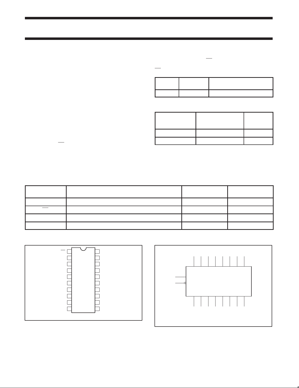
PIN CONFIGURATION
20
19
18
17
16
15
14
13
12
SF00346
V
Q7
D7
D6
Q6
Q5
D5
D4
CP
CC
1
MR
2
Q0
3
D0
4
D1
5
Q1
6
Q2
7
D2
8
D3
9
Q3 Q4
10 11
GND
1996 Mar 12 853–0066 16555
LOGIC SYMBOL
11
1
V
= Pin 20
CC
GND = Pin 10
2
3 4 7 8 13 14 1817
D0 D1 D2 D3 D4 D5 D6 D7
CP
MR
Q0 Q1 Q2 Q3 Q4 Q5 Q6 Q7
2 5 6 9 12 15 16 19
SF00347

Philips Semiconductors Product specification
74F273AOctal D flip–flop
LOGIC SYMBOL (IEEE/IEC)
1
11
32
4
7
8
13
14
17
18
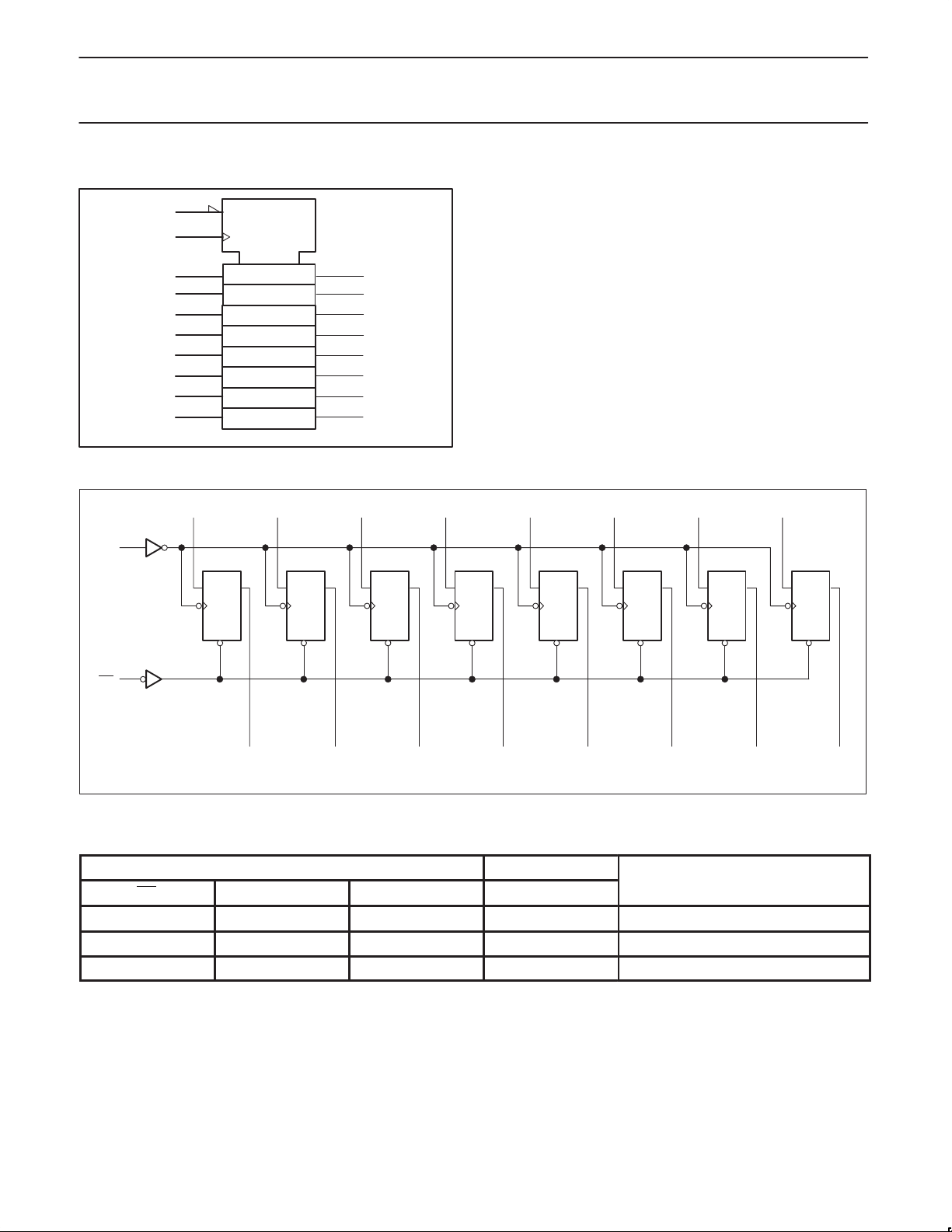
LOGIC DIAGRAM
D0
11
CP
R
C1
1D
D1
3
Q
D
CP
R
D
4
D
CP
R
Q
D
5
6
9
12
15
16
19
SF00348
D2
7
D
CP
R
D
D3
8
Q
D
CP
R
D
D4
13
Q
D
CP
R
D
D5
14
Q
D
CP
R
D
D6
17
Q
D
CP
R
D
D7
18
Q
Q
D
CP
R
D
1
MR
VCC = Pin 20
GND = Pin 10
2
Q0
Q1
5
Q2
6
9
Q3
FUNCTION TABLE
INPUTS OUTPUTS OPERATING
MR CP Dn Q0 – Q7 MODE
L X X L Reset (clear)
H ↑ h H Load ”1”
H ↑ l L Load ”0”
H = High voltage level
h = High voltage level one set–up time prior to the Low–to–High clock transition
L = Low voltage level
l = Low voltage level one set–up time prior to the Low–to–High clock transition
X = Don’t care
↑ = Low–to–High clock transition
Q4
12
Q5
15
Q6
16
19
Q7
SF00349
1996 Mar 12
3
 Loading...