

Philips 74f258a DATASHEETS
INTEGRATED CIRCUITS
74F258A
Quad 2-line to 1-line selector/multiplexer,
inverting (3-State)
Product specification 1996 Jan 05
IC15 Data Handbook
Philips Semiconductors Product specification
Quad 2-line to 1-line selector/multiplexer, inverting
(3-State)
FEA TURES
•Multifunction capability
•Non-inverting data path
•3-State outputs
•See 74F257A for non-inverting version
DESCRIPTION
The 74F258A has four identical 2-input multiplexers with 3-State
outputs which select 4 bits of data from two sources under control of
a common Select (S) input. The I
Select input is Low and the I
input is High. Data appears at the outputs in inverted form.
The 74F258A is the logical implementation of a 4-pole, 2-position
switch where the position of the switch is determined by the logic
level supplied to the Select input. Outputs are forced to a High
impedance ‘‘off” state when the Output Enable input (OE
but one device must be in the High impedance state to avoid
currents that would exceed the maximum ratings if outputs are tied
together. Design of the output signals must ensure that there is no
overlap when outputs of 3-State devices are tied together.
inputs are selected when the
0n
inputs are selected when the Select
1n
) is High. All
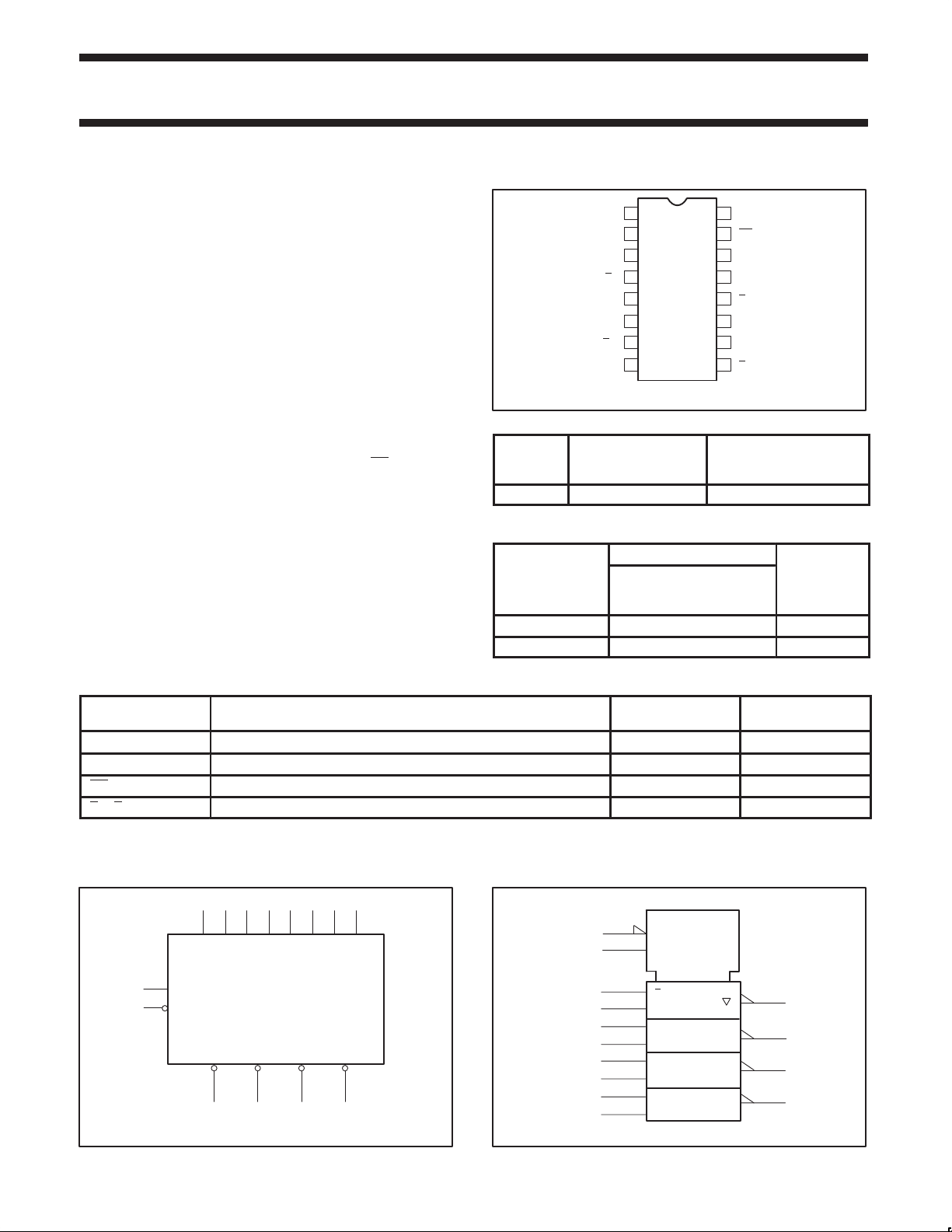
PIN CONFIGURATION
TYPE
74F258A 3.5ns 14mA
ORDERING INFORMATION
DESCRIPTION COMMERCIAL RANGE
16-pin plastic DIP N74F258AN SOT38-4
16-pin plastic SO N74F258AD SOT109-1
1
S
2
I
0a
3
I
1a
4
Y
a
5
I
0b
6
I
1b
7
Y
b
GND
TYPICAL
PROPAGATION
DELAY
ORDER CODE
VCC = 5V ±10%,
T
= 0°C to +70°C
amb
74F258A
16
V
CC
15
OE
14
I
0d
13
I
1d
12
Y
d
11
I
0c
10
I
1c
98
Y
c
SF00815
TYPICAL SUPPL Y
CURRENT (TOTAL)
PKG.
DWG. #
INPUT AND OUTPUT LOADING AND FAN-OUT TABLE
PINS DESCRIPTION
I0n, I
1n
Data inputs 1.0/1.0 20µA/0.6mA
74F(U.L.)
HIGH/LOW
S Common select input 1.0/1.0 20µA/0.6mA
OE Output Enable input (active Low) 1.0/1.0 20µA/0.6mA
Ya - Y
d
Data outputs 150/40 3.0mA/24mA
NOTE:
One (1.0) FAST Unit Load is defined as: 20µA in the High state and 0.6mA in the Low state.
LOGIC SYMBOL
1S
15
OE
VCC=Pin 16
GND=Pin 8
2 3 5 6 11 10 14 13
I
0aI1aI0bI1bI0cI1cI0dI1d
Y
Y
Y
a
b
47912
Y
c
d
SF00816
LOGIC SYMBOL (IEEE/IEC)
15
EN
1
G1
2
3
5
6
10
11
13
14
1
1
MUX
LOAD VALUE
HIGH/LOW
4
7
9
12
SF00817
1996 Jan 05 853-0361 16192
2
Philips Semiconductors Product specification
SYMBOL
PARAMETER
UNIT
Quad 2-line to 1-line selector/multiplexer, inverting
(3-State)
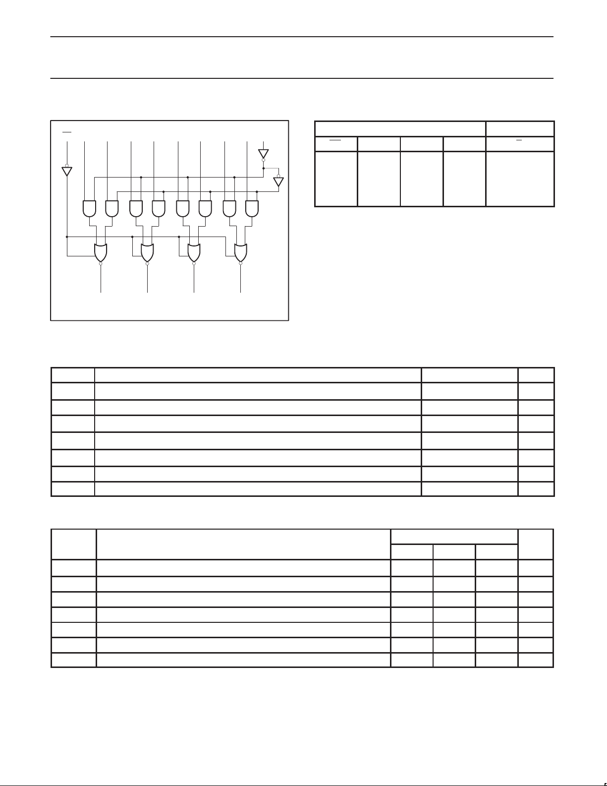
LOGIC DIAGRAM
OE
I
0aI1a
15 2 3 5 6 11 10 14 13 1
VCC=Pin 16
GND=Pin 8
Y
I
0bI1b
47912
a
Y
I
0cI1c
b
Y
I
0dI1d
c
S
Y
d
SF00818
FUNCTION TABLE
OE S I
H X X X Z
L H X L H
L H X H L
L L L X H
L L H X L
H = High voltage level
L = Low voltage level
X = Don’t care
Z = High impedance “off” state
74F258A
INPUTS OUTPUT
0
I
1
Y
ABSOLUTE MAXIMUM RATINGS
(Operation beyond the limit set forth in this table may impair the useful life of the device.
Unless otherwise noted these limits are over the operating free-air temperature range.)
SYMBOL
V
CC
V
IN
I
IN
V
OUT
I
OUT
T
amb
T
stg
Supply voltage
Input voltage –0.5 to +7.0 V
Input current
Voltage applied to output in High output state
Current applied to output in Low output state
Operating free-air temperature range 0 to +70 °C
Storage temperature range –65 to +150 °C
PARAMETER RATING UNIT
RECOMMENDED OPERATING CONDITIONS
Supply voltage
CC
High-level input voltage 2.0 V
IH
Low-level input voltage 0.8 V
IL
Input clamp current –18 mA
IK
High-level output current –3 mA
Low-level output current 24 mA
Operating free-air temperature range 0 70 °C
T
V
V
I
V
I
OH
I
OL
amb
–0.5 to +7.0 V
–30 to +5 mA
–0.5 to V
CC
48 mA
LIMITS
MIN NOM MAX
4.5 5.0 5.5 V
V
1996 Jan 05
3
 Loading...