

Philips 74f257a DATASHEETS
INTEGRATED CIRCUITS
74F257A
Quad 2-line to 1-line selector/multiplexer,
non-inverting (3-State)
Product specification 1995 Mar 31
IC15 Data Handbook
Philips Semiconductors
Philips Semiconductors Product specification
DRAWING
Quad 2-line to 1-line selector/multiplexer, non-inverting
(3-State)
FEA TURES
•Industrial range available (–40°C to +85°C)
•Multifunction capability
•Non-inverting data path
•3-State outputs
•See 74F258A for inverting version
DESCRIPTION
The 74F257A has four identical 2-input multiplexers with 3-State
outputs which select 4 bits of data from two sources uncer control of
a common Select (S) input. The I0a inputs are selected when the
common Select input is Low and the I1n inputs are selected when
the common Select input is High. Data appears at the outputs in true
non-inverted form from the selected inputs. The 74F257A is the logic
implementation of a 4-pole, 2-position switch where the position of
the switch is determined by the logic levels supplied to the common
Slect input. Outputs are forced to a high impedance “off” state when
the Output Enable (OE
impedance state to avoid currents that would exceed the maximum
rating if the outputs were tied together. Design of the Output Enable
signals must ensure that there is no overlap when outputs of 3-state
devices were tied together.
) is High. All but one device must be in high
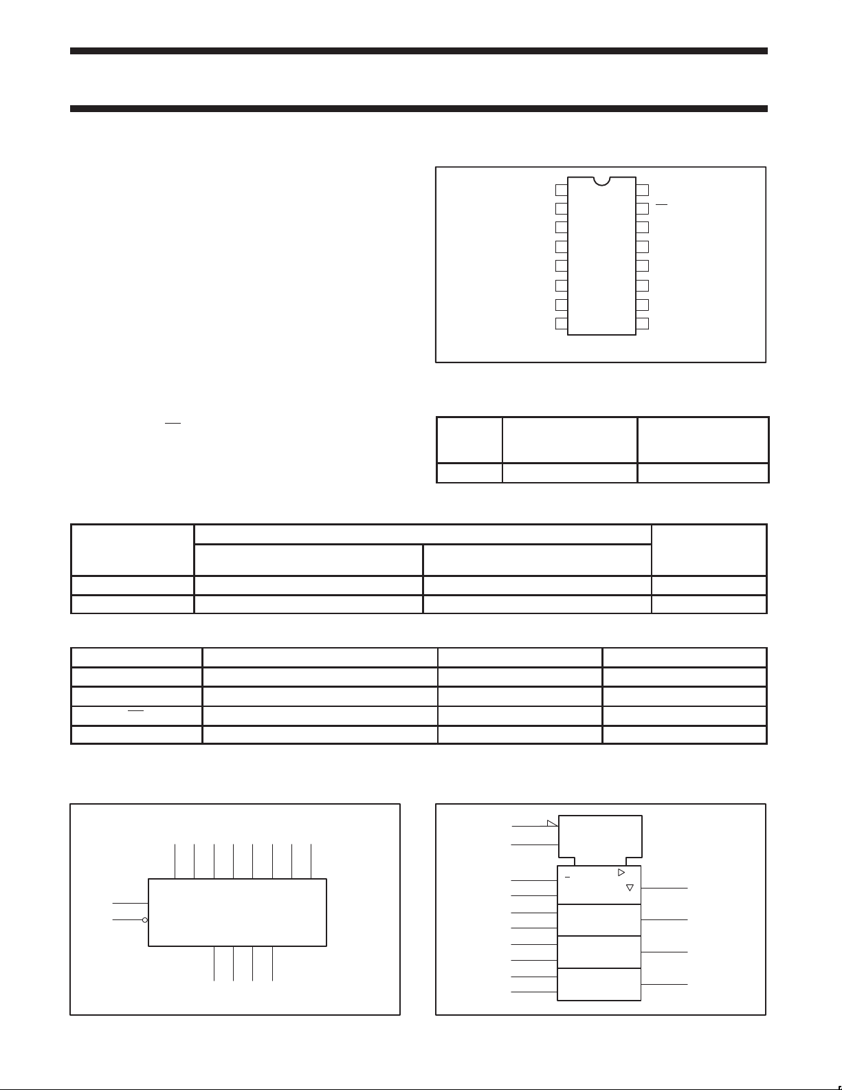
PIN CONFIGURATION
S
I0a
I1a
Ya
I0b
I1b
Yb
TYPE
74F257A 4.3ns 12mA
TYPICAL
PROPAGATION DELAY
74F257A
1
2
3
4
5
6
16
V
CC
15
OE
14
I0d
13
I1d
Yd
12
I0c
11
107
I1c
98GND Yc
SF00673
TYPICAL
SUPPLY CURRENT
(TOTAL)
ORDERING INFORMATION
ORDER CODE
DESCRIPTION
COMMERCIAL RANGE
VCC = 5V ±10%, T
= 0°C to +70°C
amb
VCC = 5V ±10%, T
INDUSTRIAL RANGE
= –40°C to +85°C
amb
16-pin plastic DIP N74F257AN I74F257AN SOT38-4
16-pin plastic SO N74F257AD I74F257AD SOT109-1
INPUT AND OUTPUT LOADING AND FAN-OUT TABLE
PINS DESCRIPTION 74F (U.L.) HIGH/LOW LOAD VALUE HIGH/LOW
I0n, I1n Data inputs 1.0/1.0 20µA/0.6mA
S Common Select input 1.0/1.0 20µA/0.6mA
OE Output Enable input (active Low) 1.0/1.0 20µA/0.6mA
Ya – Yd Data outputs 150/33 3.0mA/20mA
NOTE:
One (1.0) FAST unit load is defined as: 20µA in the High state and 0.6mA in the Low state.
LOGIC SYMBOL
1
15
VCC = Pin 16
GND = Pin 8
S
OE
2356111014
I0a I1a I0b I1b I0c I1c I0d
Ya Yb Yc Yd
47912
SF00674
13
I1d
LOGIC SYMBOL (IEEE/IEC)
15
1
2
3
5
6
10
11
13
14
EN
G1
1
1
MUX
4
7
9
12
SF00675
NUMBER
1995 Mar 31 853–0360 15059
2
Philips Semiconductors Product specification
Quad 2-line to 1-line selector/multiplexer, non-inverting
(3-State)
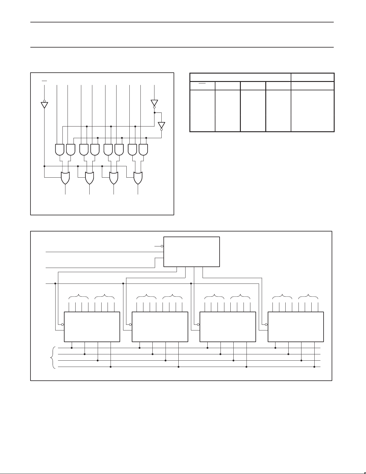
LOGIC DIAGRAM
I0a I1a I0b I1b I0c I1c I0d I1dOE S
2 3 5 6 11 10 14 1315 1
47912
Ya Yb Yc Yd
= Pin 16
V
CC
GND = Pin 8
SF00676
FUNCTION TABLE
OE S I0 I1 Y
H X X X Z
L H X L L
L H X H H
L L L X L
L L H X H
H = High voltage level
L = Low voltage level
X = Don’t care
Z = High impedance “off” state
74F257A
INPUTS OUTPUT
APPLICATION
S2
S1
S0
4-BIT
DATA
BUS
ENABLE
WORD A WORD B WORD C WORD D WORD E WORD F WORD G WORD H
I0a I1a I0b I1b I0c I1c I0d I1d
OE
S
Ya Yb Yc Yd
I0a I1a I0b I1b I0c I1c I0d I1d
OE
S
Ya Yb Yc Yd
C
B
A
Y0 Y1 Y2 Y3
74F139
I0a I1a I0b I1b I0c I1c I0d I1d
OE
S
Ya Yb Yc Yd
I0a I1a I0b I1b I0c I1c I0d I1d
OE
S
74F257A74F257A74F257A74F257A
Ya Yb Yc Yd
SF00677
1995 Mar 31
3
 Loading...