

Philips 74f244, 74f244b DATASHEETS
INTEGRATED CIRCUITS
74F244/74F244B
Octal buffers (3-State)
Product specification 1994 Dec 05
IC15 Data Handbook
Philips Semiconductors
Philips Semiconductors Product specification
PKG DWG #
74F244/74F244BOctal buffers (3-State)
FEA TURES
•Octal bus interface
• 3-State output buffer sink 64mA
•15mA source current
•Guaranteed output skew less than 2.0ns (74F244B)
•Reduced ground bounce (74F244B)
•Reduced I
•Reduced loading (74F244B I
(74F244B)
CC
= 40µA)
IL
•Split lead frame offers increased noise immunity (74F244B)
•Industrial temperature range available (-40°C to +85°C) for
74F244
DESCRIPTION
The 74F244 is an octal buffer that is ideal for driving bus lines of
buffer memory address registers. The outputs are all capable of
sinking 64mA and sourcing up to 15mA, producing very good
capacitive drive characteristics. The device features two output
enables, OE
The 74F244B is functionally equivalent to the 74F244. It has been
designed to reduce effects of ground noise. Other advantages are
noted in the features.
a and OEb, each controlling four of the 3-State outputs.
TYPE
TYPICAL
PROPAGATION
DELAY
TYPICAL SUPPL Y
CURRENT (TOTAL)
74F244 4.0ns 53mA
74F244B 4.0ns 33mA
•74F244 available in SSOP Type II package
ORDERING INFORMATION
ORDER CODE
COMMERCIAL RANGE INDUSTRIAL RANGE
DESCRIPTION
20-pin plastic DIP N74F244N, N74F244BN I74F244N SOT146-1
20-pin plastic SOL N74F244D, N74F244BD I74F244D SOT163-1
20-pin plastic SSOP II N74F244DB SOT339-1
VCC = 5V ±10%, VCC = 5V ±10%,
T
= 0°C to +70°C T
amb
= -40°C to +85°C
amb
INPUT AND OUTPUT LOADING AND FAN OUT TABLE
PINS DESCRIPTION
Ian, Ibn Data inputs (74F244) 1.0/2.67 20µA/1.6mA
Data inputs (74F244B) 1.0/0.067 20µA/40µA
OEa, OEb Output enable inputs (active low) (74F244) 1.0/1.67 20µA/1.0mA
Output enable inputs (active low) (74F244B) 1.0/0.067 20µA/40µA
Yan, Ybn Data outputs 750/106.7 15mA/64mA
NOTE: One (1.0) FAST unit load is defined as: 20µA in the high state and 0.6mA in the low state.
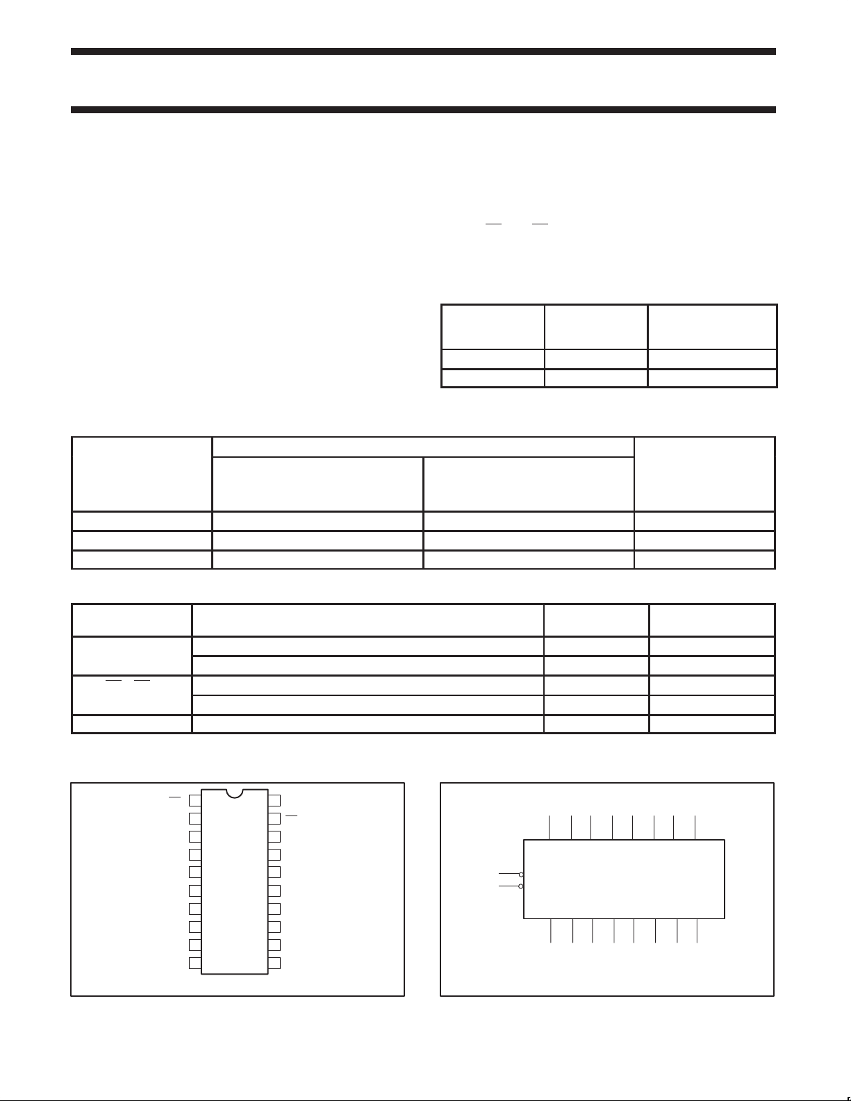
PIN CONFIGURATION
1
OEa
2
Ia0
3
Yb0
4
Ia1
5
Yb1
6
Ia2
7
Yb2
8
Ia3
9
Yb3
10 11
GND
20
V
19
OEb
18
Ya0
17
Ib0
16
Ya1
15
Ib1
14
Ya2
13
Ib2
12
Ya3
Ib3
SF00227
CC
LOGIC SYMBOL
1
= Pin 20
V
CC
GND = Pin 10
74F (U.L.)
HIGH/LOW
2 4 6 8 17 15 13 11
Ia0 Ia1 Ia2 Ia3 Ib0 Ib1 Ib2 Ib3
OEa
OEb19
Ya0 Ya1 Ya2 Ya3 Yb0 Yb1 Yb2 Yb3
18 16 14 12 3 5 7 9
LOAD VALUE
HIGH/LOW
SF00228
1994 Dec 5 853-0357 14381
2

Philips Semiconductors Product specification
74F244/74F244BOctal buffers (3-State)
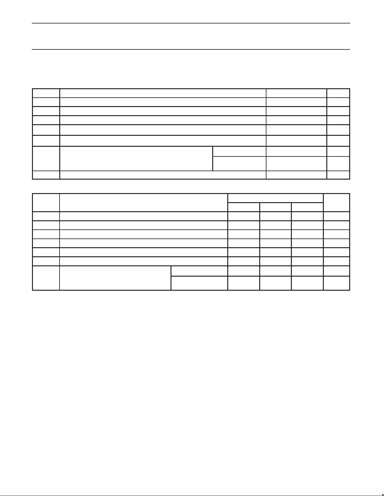
IEC/IEEE SYMBOL
1
19
2
4
6
8
17
15
13
11
LOGIC DIAGRAM
2
Ia0
4
Ia1
6
Ia2
FUNCTION TABLE
EN1
EN2
2D
OEa Ia OEb Ib Ya Yb
L L L L L L
SF00229
18
16
14
12
3
5
7
9
L H L H H H
H X H X Z Z
NOTES:
H = High voltage level
L = Low voltage level
X = Don’t care
Z = High impedance ”off” state
1
2
INPUTS OUTPUTS
18
Ya0
16
Ya1
14
Ya2
Ib0
Ib1
Ib2
17
15
13
3
Yb0
5
Yb1
7
Yb2
Ia3
OEa
V
= Pin 20
CC
GND = Pin 10
8
1
12
Ya3
Ib3
OEb
11
19
9
SF00230
Yb3
1994 Dec 5
3
Philips Semiconductors Product specification
SYMBOL
PARAMETER
UNIT
74F244/74F244BOctal buffers (3-State)
ABSOLUTE MAXIMUM RATINGS
(Operation beyond the limit set forth in this table may impair the useful life of the device. Unless otherwise noted these limits are over the
operating free air temperature range.)
SYMBOL
V
V
I
IN
V
I
OUT
T
T
CC
IN
OUT
amb
stg
Supply voltage -0.5 to +7.0 V
Input voltage -0.5 to +7.0 V
Input current -30 to +5 mA
Voltage applied to output in high output state -0.5 to V
Current applied to output in low output state 128 mA
Operating free air temperature range
Storage temperature range -65 to +150
RECOMMENDED OPERATING CONDITIONS
V
V
V
I
I
i
T
CC
IN
IL
IK
OH
ol
amb
Supply voltage 4.5 5.0 5.5 V
High-level input voltage 2.0 V
Low-level input voltage 0.8 V
Input clamp current –18 mA
High-level output current –15 mA
Low-level output current 64 mA
Operating free air temperature range
PARAMETER RATING UNIT
V
°C
°C
Commercial range 0 to +70
Industrial range
(74F244 only)
-40 to +85
CC
°C
LIMITS
MIN NOM MAX
Commercial range 0 +70
Industrial range
(74F244 only)
–40 +85
°C
°C
1994 Dec 5
4
 Loading...