Philips 74f225 DATASHEETS

INTEGRATED CIRCUITS
74F225
16X5 asynchronous FIFO (3-State)
Product specification
IC15 Data Handbook
1992 Jun 15

Philips Semiconductors Product specification
74F22516 × 5 asynchronous FIFO (3-State)
FEA TURES
•Independent synchronous inputs and outputs
•Organized as 16 words of 5 bits
Ready (IR), Unload Clock Output (UNCPOUT) and Output Ready
(OR). The data outputs are non–inverting with respect to the data
inputs and are disabled when the OE
Low, the data outputs are enabled to function as totem–pole outputs.
•DC to 25MHz data rate
•3–State outputs
•Cascadable in word–width and depth direction
DESCRIPTION
This 80–bit active element First–In–First–Out (FIFO) is a monolithic
Schottky–clamped transistor–transistor logic (STTL) array organized
as 16–words of 5–bits each. A memory system using the ’F225 can
be easily expanded in multiples of 16–words of 5–bits as shown in
Figure 1. The 3–State outputs controlled by a single enable input
(OE
) make bus connection and multiplexing simple. The ’F225
processes data in a parallel format at any desired clock rate from
DC to 25MHz. Status of the ’F225 is provided by three outputs, Input
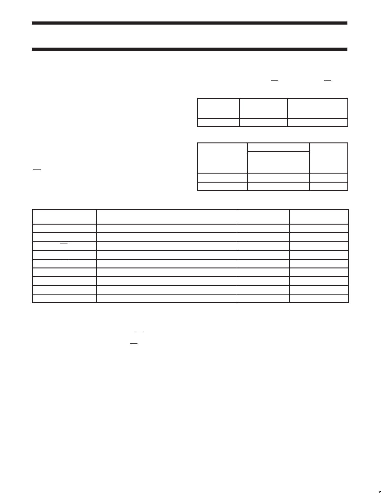
INPUT AND OUTPUT LOADING AND FAN OUT TABLE
PINS DESCRIPTION 74F (U.L.)
CPA, CPB Load clock A and load clock B inputs 1.0/0.033 20µA/20µA
D0 – D4 Data inputs 1.0/0.033 20µA/20µA
OE Output enable input (active–Low) 1.0/0.033 20µA/20µA
UNCPIN Unload clock input 1.0/0.033 20µA/20µA
MR Master reset input (active–Low) 1.0/0.033 20µA/20µA
IR Input ready output 50/33 1.0mA/20mA
UNCPOUT Unload clock output (active–Low) 50/33 1.0mA/20mA
Q0 – Q4 Data outputs 150/40 3.0mA/24mA
OR Output ready output 50/33 1.0mA/20mA
NOTE: One (1.0) FAST unit load is defined as: 20µA in the High state and 0.6mA in the Low state.
TYPE
74F225 25MHz 65mA
ORDERING INFORMATION
DESCRIPTION COMMERCIAL RANGE
20–pin plastic DIP N74F225N SOT146-1
20–pin plastic SOL N74F225D SOT163-1
TYPICAL f
ORDER CODE
V
CC
T
= 0°C to +70°C
amb
HIGH/LOW
input is High. When OE is
TYPICAL SUPPL Y
MAX
= 5V ±10%,
CURRENT
( TOTAL)
LOAD VALUE
HIGH/LOW
PKG DWG #
RESET MODE
A High–to–Low transition on the Master Reset (MR) input invalidates
all data stored in the FIFO by clearing the control logic and setting
OR Low. This High–to–Low transition on the MR
effect the data outputs but since OR is driven Low, it signifies invalid
data on the outputs.
input does not
READ MODE
The Output Ready (OR) output is High when valid data is present on
the data outputs. Data in the array is shifted on the Low–to–High
transition of the Unload Clock Input (UNCPIN). In order for Output
Ready (OR) to go High, Unload Clock Input (UNCPIN) must also be
High.
WRITE MODE
Data may be written into the array on the Low–to–High transition of
either load clock (CPA or CPB) input. When writing data into the
FIFO, one of the load clock inputs must be held High while the other
strobes data into the FIFO. This arrangement allows either load
clock to function as an inhibit for the other. Input Ready (IR)
monitors the status of the last word location and signifies when the
FIFO is full. This output is High whenever the FIFO is available to
accept new data. The unload clock output (UNCPOUT) also
monitors the last word location. This output generates a
Low–logic–level pulse (synchronized to the internal clock pulse)
when the last word location is vacant
June 15, 1992 853-1652 06992
2

Philips Semiconductors Product specification
74F22516 × 5 asynchronous FIFO (3-State)
PIN CONFIGURATION
CPA
1
IR
2
UNCPOUT
3
D0
4
D1
5
6
D2
D3
7
D4
8
9
OE
10 11
GND
LOGIC SYMBOL
CPA
1
CPB
19
UNCPIN
16
OE
9
MR
18
Q0 Q1 Q2 Q3 Q4 IR OR
4 5 6 7 8
D0 D1 D2 D3 D4
UNCPOUT
20
19
18
17
16
15
14
13
12
SF00334
V
CC
CPB
MR
OR
UNCPIN
Q0
Q1
Q2
Q3
Q4
IEC/IEEE SYMBOL
EN5
CT=0
CT<16
CT>0
1D
FIFO 16 X
5
CTR
&
1
&
–
Z4
+
G1
G2/Z3
2CT<16
5
3
3
2
17
4
15
14
13
12
11
SF00336
9
18
1
19
16
4
5
6
7
8
3
V
CC
GND
= Pin 20
= Pin 10
15 14 13 12 11 2 17
SF00335
June 15, 1992
3

Philips Semiconductors Product specification
74F22516 × 5 asynchronous FIFO (3-State)
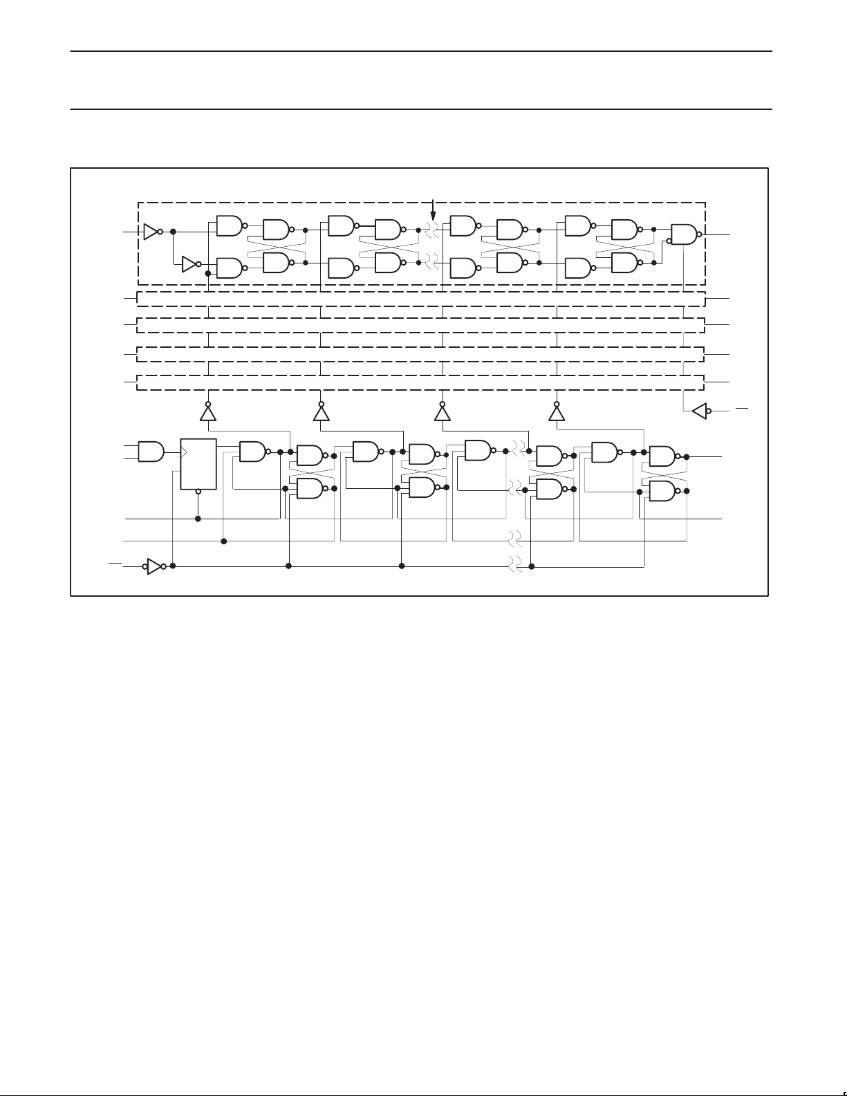
LOGIC DIAGRAM
Word 16
(last word)
Detail A
4
D0
Word 15
Word 3–14
same as 2 or 16
Word 2
Word 1
(first word)
15
QO
UNC-
POUT
D1
D2
D3
D4
CPA
CPB
IR
MR
5
6
7
8
1
19
3
2
18
D
CP
CLR
Q
Detail A
Detail A
Detail A
Detail A
14
13
12
11
9
17
OR
16
UNCPIN
V
= pin 20
CC
GND = pin 10
SF00337
Q1
Q2
Q3
Q4
OE
June 15, 1992
4

Philips Semiconductors Product specification
74F22516 × 5 asynchronous FIFO (3-State)
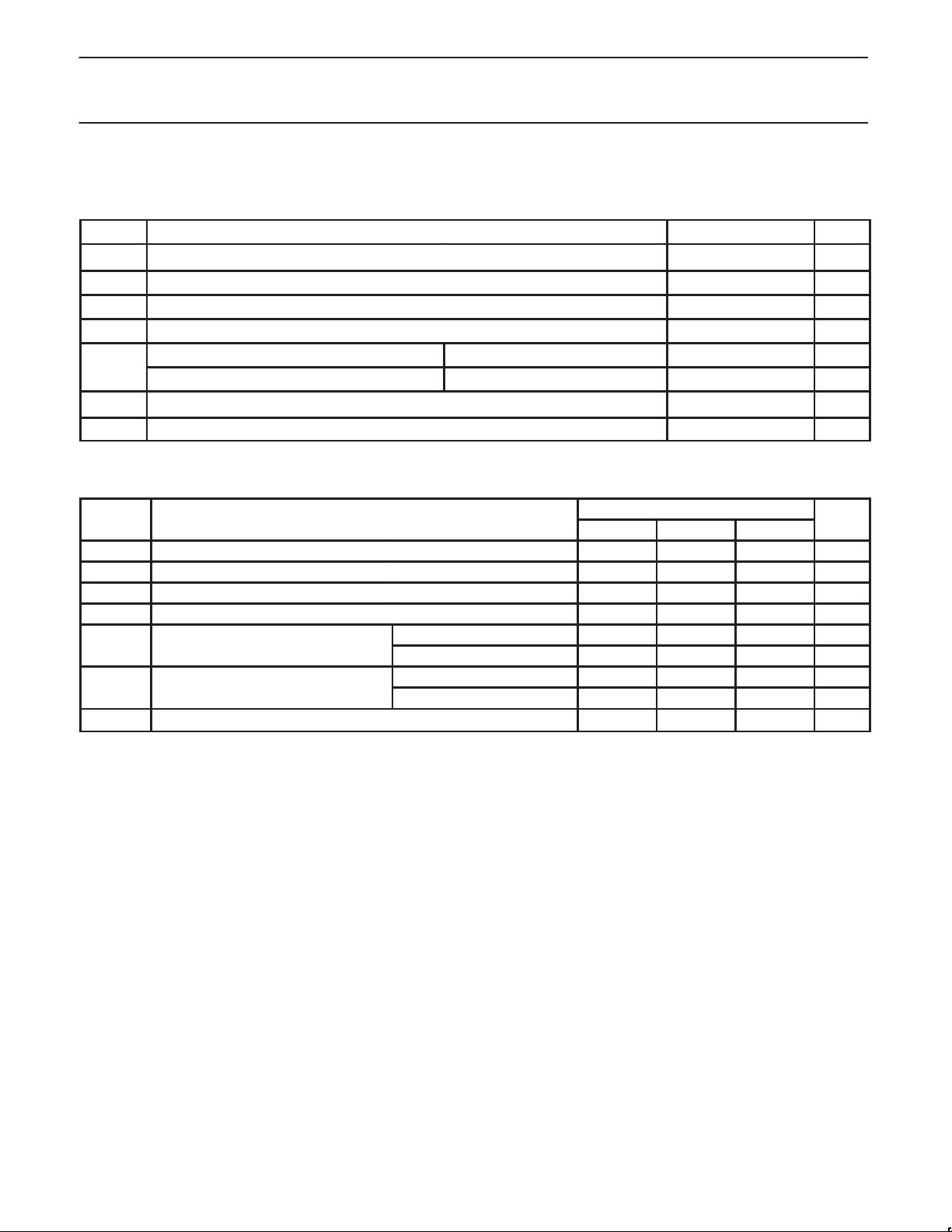
ABSOLUTE MAXIMUM RATINGS
(Operation beyond the limit set forth in this table may impair the useful life of the device. Unless otherwise noted these limits are over the
operating free air temperature range.)
SYMBOL PARAMETER RATING UNIT
V
V
V
I
OUT
T
T
RECOMMENDED OPERATING CONDITIONS
SYMBOL PARAMETER LIMITS UNIT
V
T
Supply voltage
CC
Input voltage –0.5 to +7.0 V
IN
I
Input current –30 to +5 mA
IN
Voltage applied to output in High output state –0.5 to V
OUT
–0.5 to +7.0 V
Current applied to output in Low output state IR, OR, UNCPOUT 40 mA
Current applied to output in Low output state Data outputs 48 mA
Operating free air temperature range 0 to +70
amb
Storage temperature range –65 to +150
stg
MIN NOM MAX
Supply voltage 4.5 5.0 5.5 V
CC
V
V
I
I
OH
High–level input voltage 2.0 V
IN
Low–level input voltage 0.8 V
IL
Input clamp current –18 mA
Ik
High–level output current IR, OR, UNCPOUT –1 mA
Data outputs –3 mA
I
OL
Low–level output current IR, OR, UNCPOUT 20 mA
Data outputs 24 mA
amb
Operating free air temperature range 0 +70
CC
V
°C
°C
°C
June 15, 1992
5
 Loading...