

Page 1

Philips Semiconductors FAST Products Product specification
74F1998-bit parallel-access shift register
1
June 15, 1988 853–0082 93568
FEATURES
•Buffered clock and control inputs
•Shift right and parallel load capability
•Fully synchronous data transfers
•J-K(D) inputs to first stage
•Clock enable for hold (do nothing) mode
•Asynchronous Master Reset
DESCRIPTION
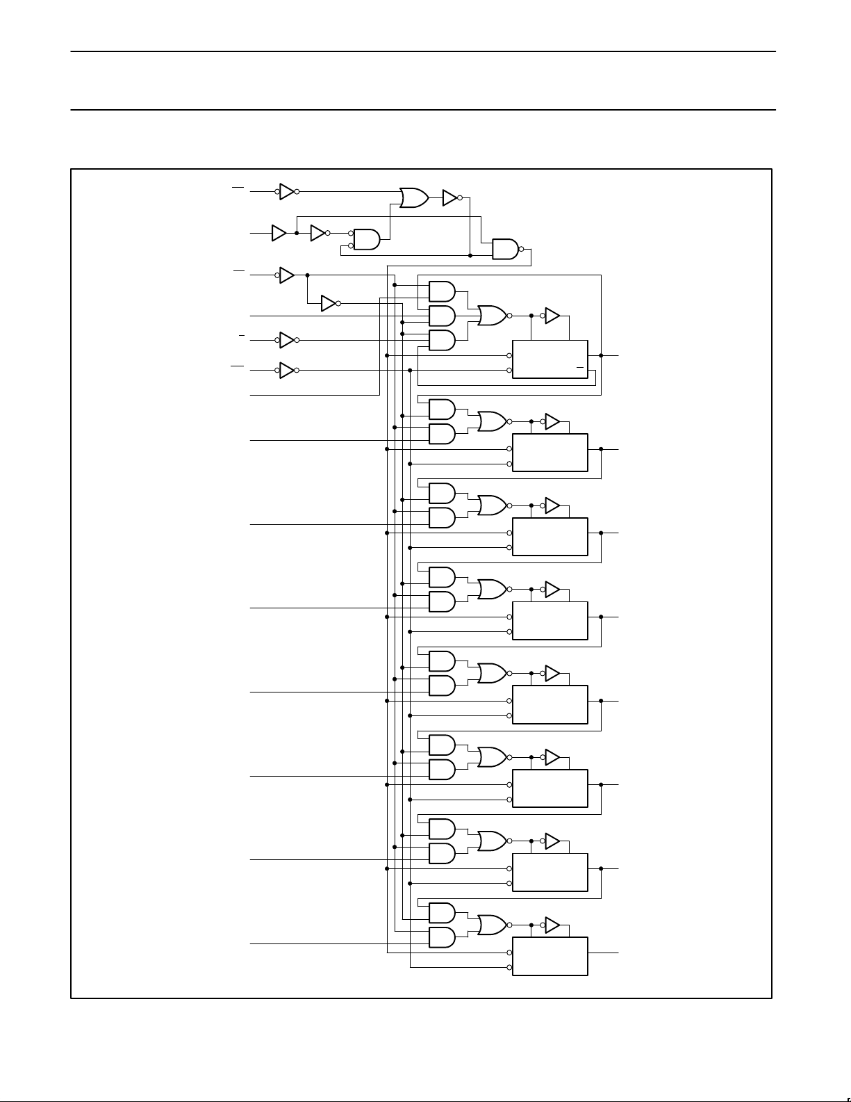
The 74F199 is an 8-bit Parallel Access Shift Register and its
functional characteristics are indicated in the Logic Diagram and
Function Table. The device is useful in a variety of shifting, counting
and storage applications. It performs serial, parallel, serial-to-parallel,
or parallel–to-serial data transfers at very high speeds.
The 74F199 operates in two primary modes: shift right (Q0→Q1)
and parallel load, which are controlled by the state of the Parallel
Enable (PE
) input. Serial data enters the first flip-flop (Q0) via the J
and K
inputs when the PE input is High, and is shifted one bit in the
direction Q0→Q1→Q2 following each Low-to-High clock transition.
The J and K
inputs provide the flexibility of the J-K type input for
special applications, and by tying the two together the simple D-type
input is made for general applications.
The device appears as eight common clocked D flip-flops when the
PE
input is Low. After the Low-to-High clock transition, data on the
parallel inputs (D0–D7) is transferred to the respective Q0–Q7
outputs.
All parallel and serial data transfers are synchronous, occurring after
each Low-to-High clock transition. The 74F199 utilizes
edge-triggered, therefore there is no restriction on the activity of the
J, K
, Dn, and PE inputs for logic operation, other than the setup and
hold time requirements.
A Low on the Master Reset (MR
) input overrides all other inputs and
clears the register asynchronously forcing all bit positions to a Low
state.
PIN CONFIGURATION
SF00152
1
2
3
4
5
6
7
8
9
10
11
12 13
14
15
16
17
18
19
20
21
22
23
24
K
J
D0
Q0
D1
Q1
D2
Q2
D3
Q3
CE
V
CC
PE
D7
Q7
D6
Q6
D5
D4
Q5
Q4
MR
CP
GND
TYPE TYPICAL f
MAX
TYPICAL
SUPPLY CURRENT
(TOTAL)
74F199 95MHz 70mA
ORDERING INFORMATION
DESCRIPTION
COMMERCIAL RANGE
V
CC
= 5V ±10%, T
amb
= 0°C to +70°C
24-pin plastic slim DIP
(300mil)
N74F199N
24-pin plastic SOL N74F199D
INPUT AND OUTPUT LOADING AND FAN-OUT TABLE
PINS DESCRIPTION 74F (U.L.) HIGH/LOW LOAD VALUE HIGH/LOW
D0–D7 Parallel data inputs 1.0/1.0 20µA/0.6mA
J, K J and K inputs 1.0/1.0 20µA/0.6mA
PE Parallel Enable input 1.0/1.0 20µA/0.6mA
CE Clock Enable input 1.0/1.0 20µA/0.6mA
DP Clock Pulse inputs (Active rising edge) 1.0/1.0 20µA/0.6mA
MR Master Reset input (Active Low) 1.0/1.0 20µA/0.6mA
Q0–Q7 Data outputs 50/33 1.0mA/20mA
NOTE: One (1.0) FAST unit load is defined as: 20µA in the High state and 0.6mA in the Low state.
查询74F199供应商查询74F199供应商
Page 2

Philips Semiconductors FAST Products Product specification
74F1998-bit parallel-access shift register
June 15, 1988
2
LOGIC SYMBOL
Q0 Q1 Q2 Q3
4 6 8 10
V
CC
= Pin 24
GND = Pin 12
23
2
1
13
11
14
PE
J
K
CP
CE
MR
D1 D2
7 9
SF00153
D3D0
3 5
Q5 Q6 Q7
15 17 19 21
D5 D6
20 22
D7D4
16 18
Q4
IEEE/IEC SYMBOL
SF00154
1
9
16
18
20
22
1
3
5
7
2
14
23
13
11
1
&
C2/→
SRG8
C3
R
2J
2K
2, 3D
2, 3D
10
15
17
19
21
4
6
8
FUNCTION TABLE
INPUTS OUTPUTS
MR CP CE PE J K Dn Q0 Q1 … Q6 Q7
OPERATING MODES
L X X X X X X L L … L L Reset (clear
H ↑ l h h h X H q0 … q5 q6 Shift, set First stage
H ↑ l h l l X L q0 … q5 q6 Shift, reset First stage
H ↑ l h h l X q0 q0 … q5 q6 Shift, toggle First stage
H ↑ l h l h X q0 q0 … q5 q6 Shift, retain First stage
H ↑ l l X X dn d0 d1 … d6 d7 Parallel load
H ↑ h X X X X q0 q1 … q6 q7 Hold (do nothing)
H = High voltage level
h = High voltage level one setup time prior to the Low-to-High clock transition
L = Low voltage level
l = Low voltage level one setup time prior t the Low-to-High clock transition
X = Don’t care
↑ = Low-to-High clock transition
dn(qn) = Lower case letters indicate the state of the referenced input (or output) one setup time prior to the Low-to-High clock transition
Page 3
Philips Semiconductors FAST Products Product specification
74F1998-bit parallel-access shift register
June 15, 1988
3
LOGIC DIAGRAM
CP
RD
R S
Q
22
D7
21
Q7
CP
RD
R S
Q
20
D6
19
Q6
CP
RD
R S
Q
18
D5
17
Q5
CP
RD
R S
Q
16
D4
15
Q4
CP
RD
R S
Q
9
D3
10
Q3
CP
RD
R S
Q
7
D2
8
Q2
CP
RD
R S
Q
5
D1
6
Q1
CP
RD
R S
Q
4
Q0
Q
3
D0
14
MR
1
K
2
J
23
PE
13
CP
11
CE
SF00155
Page 4
Philips Semiconductors FAST Products Product specification
74F1998-bit parallel-access shift register
June 15, 1988
4
TYPICAL TIMING DIAGRAM
CP
CE
MR
K
J
H
L
SERIAL
INPUTS
PARALLEL
DATA
INPUTS
OUTPUTS
H
L
H
L
H
H
INHIBIT
H H H H H
L L L
PE
D0
D1
D2
D3
D4
D5
D6
D7
Q0
Q1
Q2
Q3
Q4
Q5
Q6
Q7
CLEAR
SERIAL SHIFT
LOAD
SERIAL SHIFT
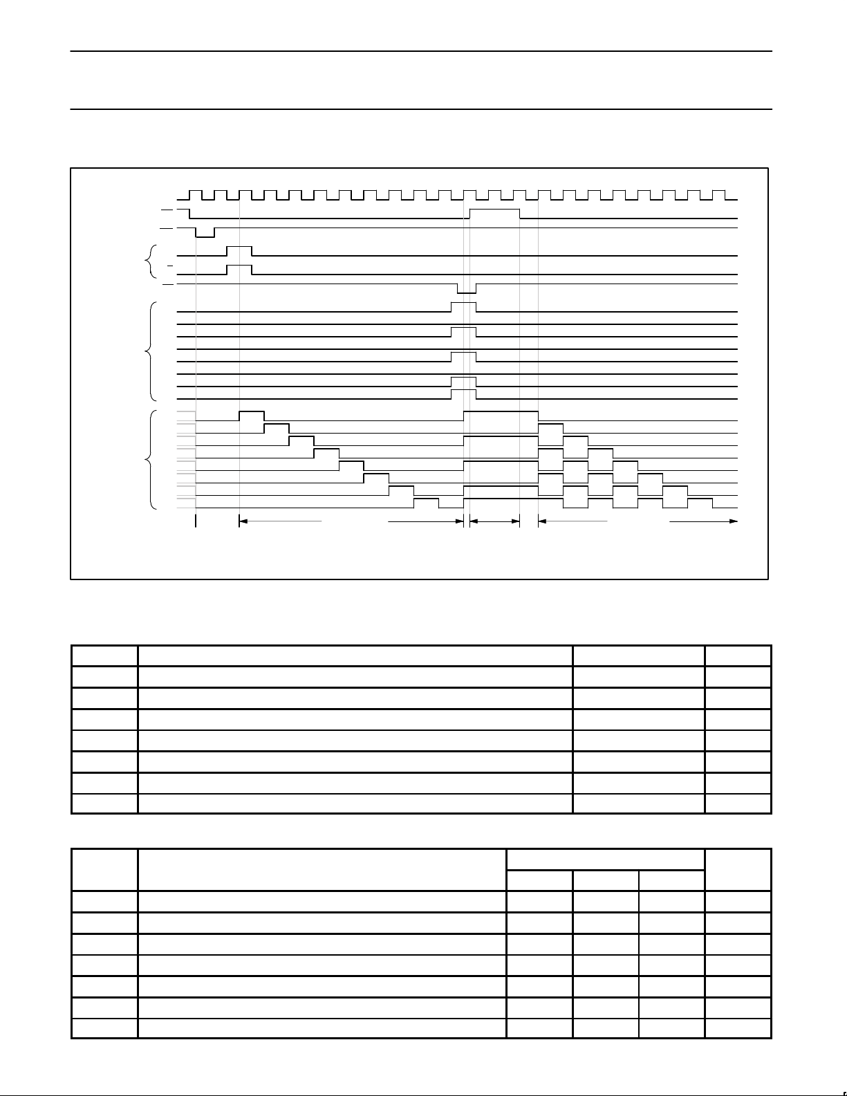
Typical Load, Serial-Shift, Inhibit and Clear Sequences
SF00156
ABSOLUTE MAXIMUM RATINGS
(Operation beyond the limits set forth in this table may impair the useful life of the device.
Unless otherwise noted these limits are over the operating free-air temperature range.)
SYMBOL
PARAMETER RATING UNIT
V
CC
Supply voltage –0.5 to +7.0 V
V
IN
Input voltage –0.5 to +7.0 V
I
IN
Input current –30 to +5 mA
V
OUT
Voltage applied to output in High output state –0.5 to V
CC
V
I
OUT
Current applied to output in Low output state 40 mA
T
amb
Operating free-air temperature range 0 to +70 °C
T
stg
Storage temperature range –65 to +150 °C
RECOMMENDED OPERATING CONDITIONS
LIMITS
SYMBOL
PARAMETER
MIN NOM MAX
UNIT
V
CC
Supply voltage 4.5 5.0 5.5 V
V
IH
High-level input voltage 2.0 V
V
IL
Low-level input voltage 0.8 V
I
IK
Input clamp current –18 mA
I
OH
High-level output current –1 mA
I
OL
Low-level output current 20 mA
T
amb
Operating free-air temperature range 0 +70 °C
Page 5
Philips Semiconductors FAST Products Product specification
74F1998-bit parallel-access shift register
June 15, 1988
5
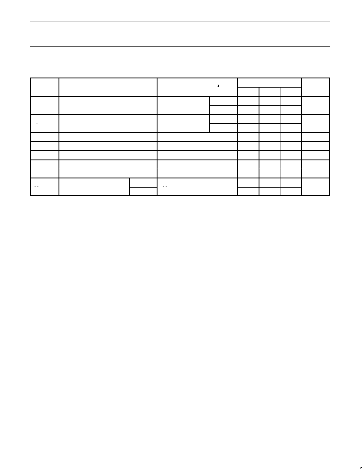
DC ELECTRICAL CHARACTERISTICS
(Over recommended operating free-air temperature range unless otherwise noted.)
LIMITS
SYMBOL
PARAMETER
TEST CONDITIONS
1
MIN TYP
2
MAX
UNIT
VCC = MIN, VIL = MAX ±10%V
CC
2.5
VOHHigh-level output voltage
VIH = MIN, IOH = MAX ±5%V
CC
2.7 3.4
V
VCC = MIN, VIL = MAX ±10%V
CC
0.35 0.50
VOLLow-level output voltage
VIH = MIN, IOL = MAX ±5%V
CC
0.35 0.50
V
V
IK
Input clamp voltage VCC = MIN, II = I
IK
–0.73 –1.2 V
I
I
Input current at maximum input voltage VCC = MAX, VI = 7.0V 100 µA
I
IH
High-level input current VCC = MAX, VI = 2.7V 20 µA
I
IL
Low-level input current VCC = MAX, VI = 0.5V –0.6 mA
I
OS
Short-circuit output current
3
VCC = MAX –60 –150 mA
I
CCH
65 90
ICCSupply current (total)
I
CCL
VCC = MAX
75 105
mA
NOTES:
1. For conditions shown as MIN or MAX, use the appropriate value specified under recommended operating conditions for the applicable type.
2. All typical values are at V
CC
= 5V, T
amb
= 25°C.
3. Not more than one output should be shorted at a time. For testing I
OS
, the use of high-speed test apparatus and/or sample-and-hold
techniques are preferable in order to minimize internal heating and more accurately reflect operational values. Otherwise, prolonged shorting
of a High output may raise the chip temperature well above normal and thereby cause invalid readings in other parameter tests. In any
sequence of parameter tests, I
OS
tests should be performed last.
Page 6
Philips Semiconductors FAST Products Product specification
74F1998-bit parallel-access shift register
June 15, 1988
6
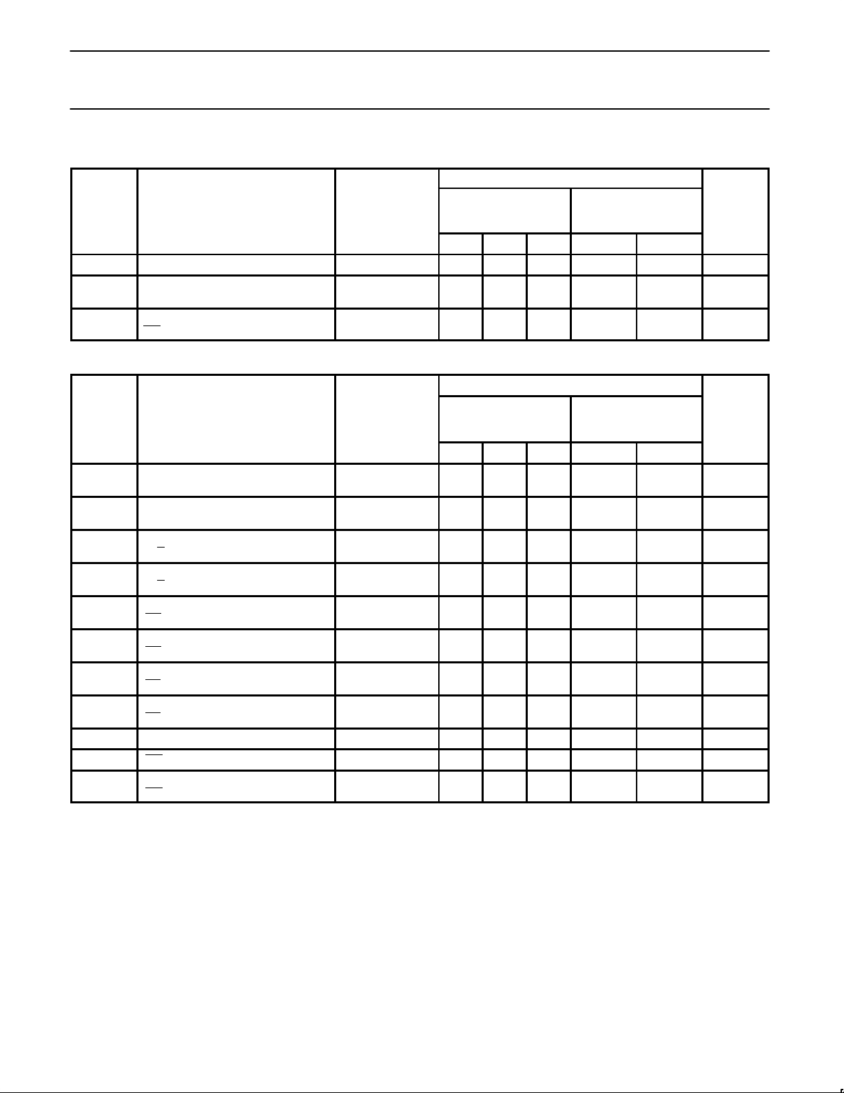
AC ELECTRICAL CHARACTERISTICS
LIMITS
SYMBOL
PARAMETER
TEST
CONDITION
VCC = +5.0V
T
amb
= +25°C
C
L
= 50pF, RL = 500Ω
VCC = +5.0V ± 10%
T
amb
= 0°C to +70°C
C
L
= 50pF, RL = 500Ω
UNIT
MIN TYP MAX MIN MAX
f
MAX
Maximum clock frequency Waveform 1 80 95 70 MHz
t
PLH
t
PHL
Propagation delay
CP to Qn
Waveform 1
5.5
6.5
8.0
9.5
11.0
12.5
4.5
3.5
12.0
13.5
ns
t
PHL
Propagation delay
MR
to Qn
Waveform 2 5.5 8.0 10.5 5.0 12.0 ns
AC SETUP REQUIREMENTS
LIMITS
SYMBOL
PARAMETER
TEST
CONDITION
VCC = +5.0V
T
amb
= +25°C
CL = 50pF, RL = 500Ω
VCC = +5.0V ± 10%
T
amb
= 0°C to +70°C
CL = 50pF, RL = 500Ω
UNIT
MIN TYP MAX MIN MAX
tS(H)
t
S
(L)
Setup time, High or Low
Dn to CP
Waveform 3
0.0
1.5
0.0
2.5
ns
th(H)
t
h
(L)
Hold time, High or Low
Dn to CP
Waveform 3
2.0
4.5
2.5
5.5
ns
ts(H)
t
s
(L)
Setup time, High or Low
J, K
to CP
Waveform 3
0.0
2.5
0.0
3.0
ns
th(H)
th(L)
Hold time, High or Low
J, K to CP
Waveform 3
0.0
3.5
0.0
4.0
ns
ts(H)
t
s
(L)
Setup time, High or Low
CE
to CP
Waveform 3
0.0
2.5
0.0
3.0
ns
th(H)
t
h
(L)
Hold time, High or Low
CE
to CP
Waveform 3
0.0
4.5
0.0
5.5
ns
ts(H)
ts(L)
Setup time, High or Low
PE to CP
Waveform 3
8.0
8.0
9.0
9.0
ns
th(H)
th(L)
Hold time, High or Low
PE to CP
Waveform 3
0.0
0.0
0.0
0.0
ns
tw(H) CP pulse width, High Waveform 1 4.5 5.5 ns
tw(L) MR pulse width, Low Waveform 2 4.0 4.5 ns
t
rec
Recovery time
MR
to CP
Waveform 2 5.5 6.5 ns
Page 7
Philips Semiconductors FAST Products Product specification
74F1998-bit parallel-access shift register
June 15, 1988
7
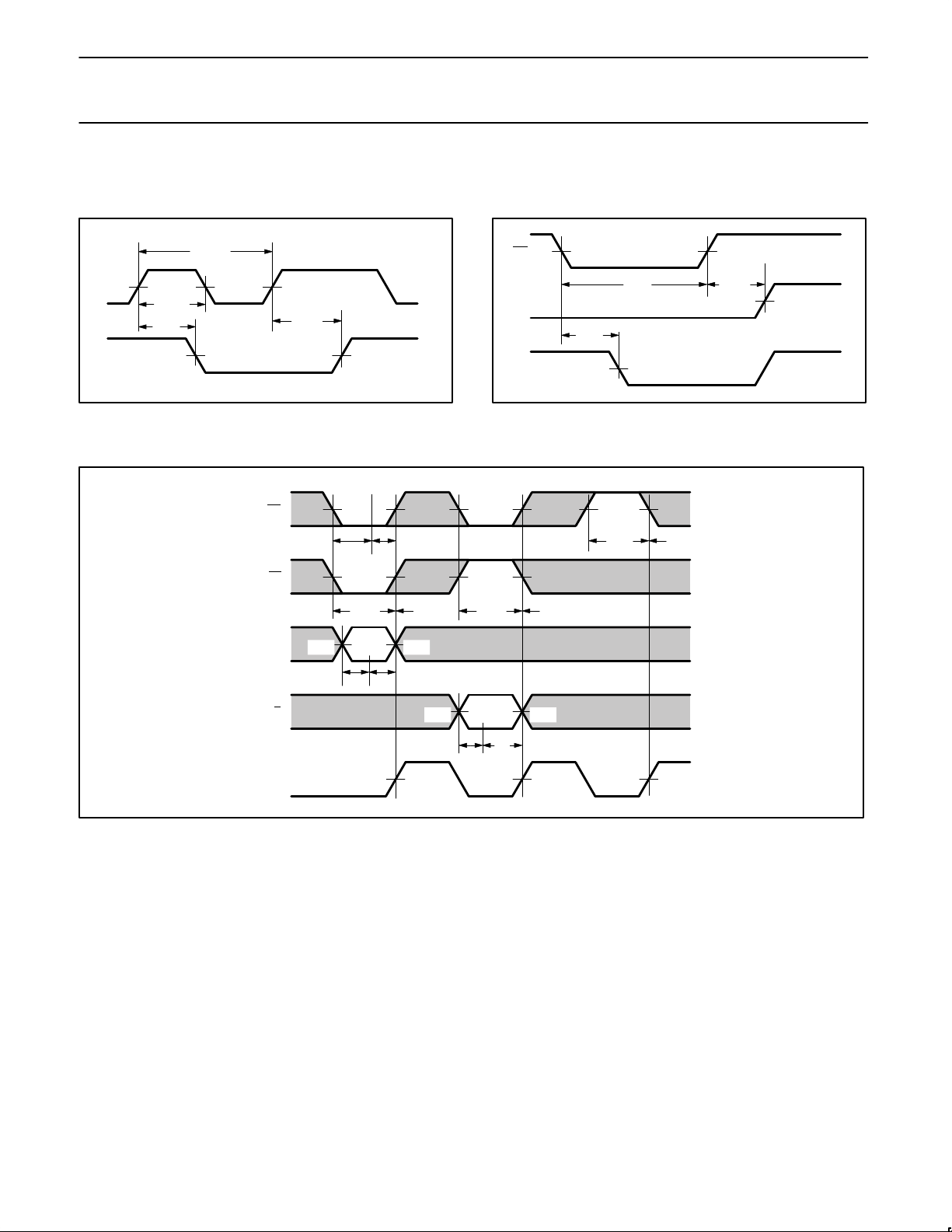
AC WAVEFORMS
For all waveforms, VM = 1.5V.
The shaded areas indicate when the input is permitted to change for predictable output performance.
V
M
SF00157
CP
Qn
V
M
tw(H)
t
PHL
V
M
t
PLH
1/f
MAX
Waveform 1. Propagation Delay, Clock Input to Output,
Clock Widths, and Maximum Clock Frequency
V
M
SF00158
MR
Qn
V
M
tw(L)
t
PHL
V
M
t
REC
CP
V
M
Waveform 2. Master Reset Pulse Width, Master Reset to
Output Delay and Master Reset to Clock Recovery Time
V
M
ts(L)
V
M
V
M
V
M
V
M
V
M
V
M
V
M
V
M
V
M
V
M
V
M
STABLE
STABLE
ts(H) th = 0
th = 0
t
h
t
s
tht
s
ts(L) th = 0
ts(L) t
h
CE
PE
Dn
J, K
CP
SF00159
Waveform 3. Setup Time and Hold Time
Page 8
Philips Semiconductors FAST Products Product specification
74F1998-bit parallel-access shift register
June 15, 1988
8
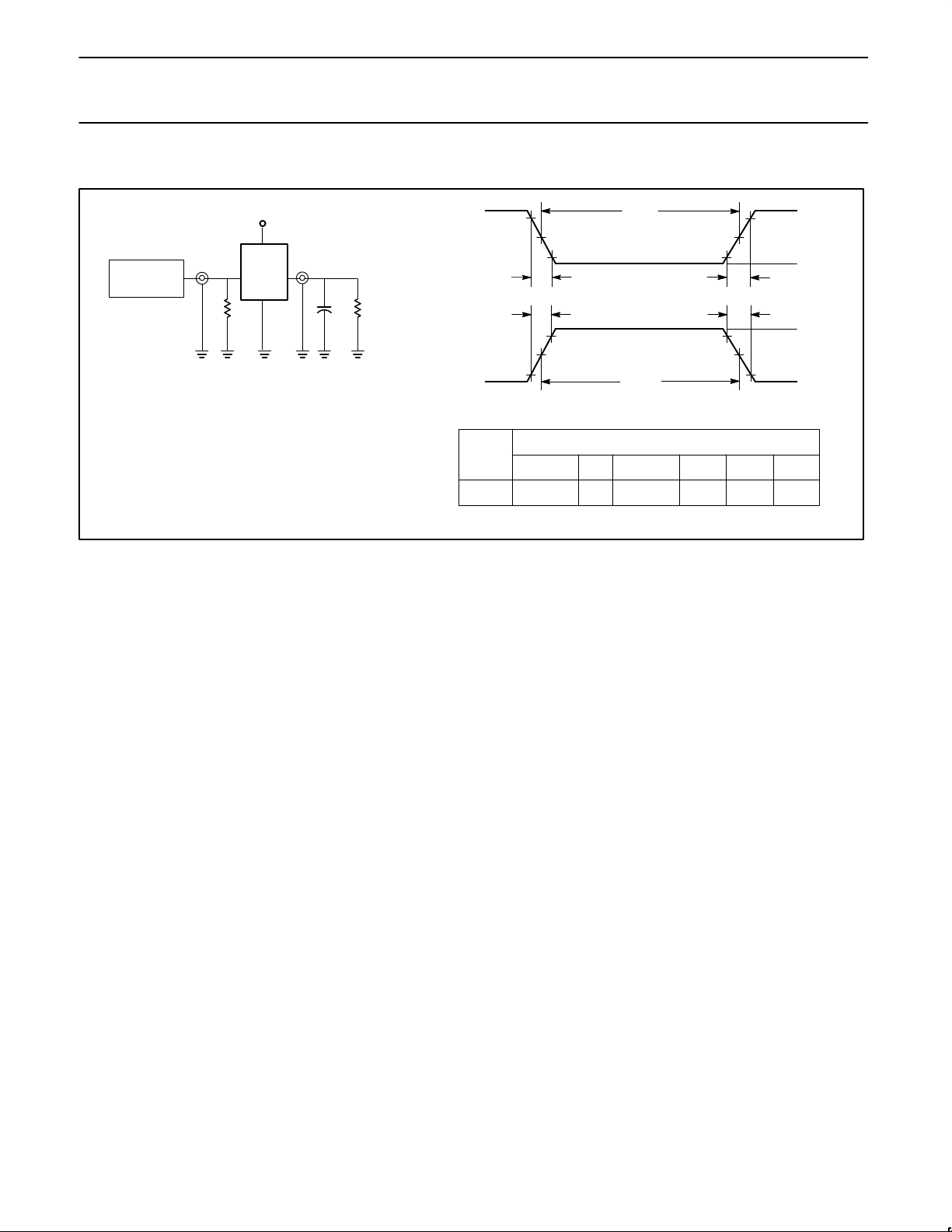
TEST CIRCUIT AND WAVEFORMS
t
w
90%
V
M
10%
90%
V
M
10%
90%
V
M
10%
90%
V
M
10%
NEGATIVE
PULSE
POSITIVE
PULSE
t
w
AMP (V)
0V
0V
t
THL (tf
)
INPUT PULSE REQUIREMENTS
rep. rate
t
w
t
TLHtTHL
1MHz 500ns
2.5ns 2.5ns
Input Pulse Definition
V
CC
family
74F
D.U.T.
PULSE
GENERATOR
R
L
C
L
R
T
V
IN
V
OUT
Test Circuit for Totem-Pole Outputs
DEFINITIONS:
R
L
= Load resistor;
see AC electrical characteristics for value.
CL= Load capacitance includes jig and probe capacitance;
see AC electrical characteristics for value.
R
T
= Termination resistance should be equal to Z
OUT
of
pulse generators.
t
THL (tf
)
t
TLH (tr
)
t
TLH (tr
)
AMP (V)
amplitude
3.0V
1.5V
V
M
SF00006
 Loading...