

Philips 74f169 DATASHEETS

INTEGRATED CIRCUITS
74F168*, 74F169
4-bit up/down binary synchronous counter
* Discontinued part. Please see the Discontinued Product List in Section 1, page 21.
Product specification 1996 Jan 05
IC15 Data Handbook
Philips Semiconductors Product specification
74F1694-bit up/down binary synchronous counter
FEA TURES
•Synchronous counting and loading
•Up/Down counting
•Modulo 16 binary counter
•Two Count Enable inputs for n-bit cascading
•Positive edge-triggered clock
•Built-in carry look-ahead capability
•Presettable for programmable operation
DESCRIPTION
The 74F169 is a 4-bit synchronous, presettable Modulo 16 up/down
counter featuring an internal carry look-ahead for applications in
high-speed counting designs. Synchronous operation is provided by
having all flip-flops clocked simultaneously so that the outputs
change coincident with each other when instructed by the Count
Enable inputs and internal gating. This mode of operation eliminates
the output spikes which are normally associated with asynchronous
(ripple clock) counters. A buffered clock input triggers the flip-flops
on the Low-to-High transition of the clock.
The counter is fully programmable; that is, the outputs may be
preset to either level.
Presetting is synchronous with the clock and takes place regardless
of the levels of the Count Enable inputs. A Low level on the Parallel
Enable (PE
D
input to be loaded into the counter on the next Low-to-High
n
transition of the clock.
The direction of counting is controlled by the Up/Down (U/D
High will cause the count to increase, a Low will cause the count to
decrease.
The carry look-ahead circuitry provides for n-bit synchronous
applications without additional gating. Instrumental in accomplishing
this function are two Count Enable inputs (CET
Terminal Count (TC) output. Both Count Enable inputs must be Low
to count. The CET
TC
duration approximately equal to the High level portion of the Q
output. The Low level TC pulse is used to enable successive
cascaded stages.
) input disables the counter and causes the data at the
) input; a
, CEP) and a
input is fed forward to enable the TC output. The
output thus enabled will produce a Low output pulse with a
0
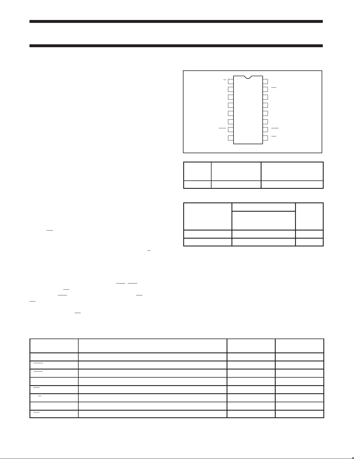
PIN CONFIGURATION
1
U/D
2
CP
3
D
0
4
D
1
5
D
2
6
D
3
CEP
7
GND
TYPE TYPICAL f
MAX
74F169 115MHz 35mA
16
V
CC
15
TC
14
Q
0
13
Q
1
12
Q
2
11
Q
3
CET
10
98
PE
SF00766
TYPICAL
SUPPLY CURRENT
(TOTAL)
ORDERING INFORMATION
ORDER CODE
DESCRIPTION
16-pin plastic DIP N74F169N SOT38-4
16-pin plastic SO N74F169D SOT109-1
COMMERCIAL RANGE
VCC = 5V ±10%,
T
= 0°C to +70°C
amb
DWG #
PKG
INPUT AND OUTPUT LOADING AND FAN-OUT TABLE
PINS DESCRIPTION
D0 - D
3
Parallel data inputs 1.0/1.0 20µA/0.6mA
74F(U.L.)
HIGH/LOW
CEP Count Enable parallel input (active Low) 1.0/1.0 20µA/0.6mA
CET Count Enable Trickle input (active Low) 1.0/2.0 20µA/1.2mA
CP Clock input (active rising edge) 1.0/1.0 20µA/0.6mA
PE Parallel Enable input (active Low) 1.0/1.0 20µA/0.6mA
U/D Up/Down count control input 1.0/1.0 20µA/0.6mA
Q0 - Q
3
Flip-flop outputs 50/33 1.0mA/20mA
TC Terminal count output (active Low) 50/33 1.0mA/20mA
NOTE: One (1.0) FAST Unit Load (U.L.) is defined as: 20µA in the High state and 0.6mA in the Low state.
1996 Jan 05 853–0350 16190
2
LOAD VALUE
HIGH/LOW
Philips Semiconductors Product specification
OPERATING MODE
74F1694-bit up/down binary synchronous counter
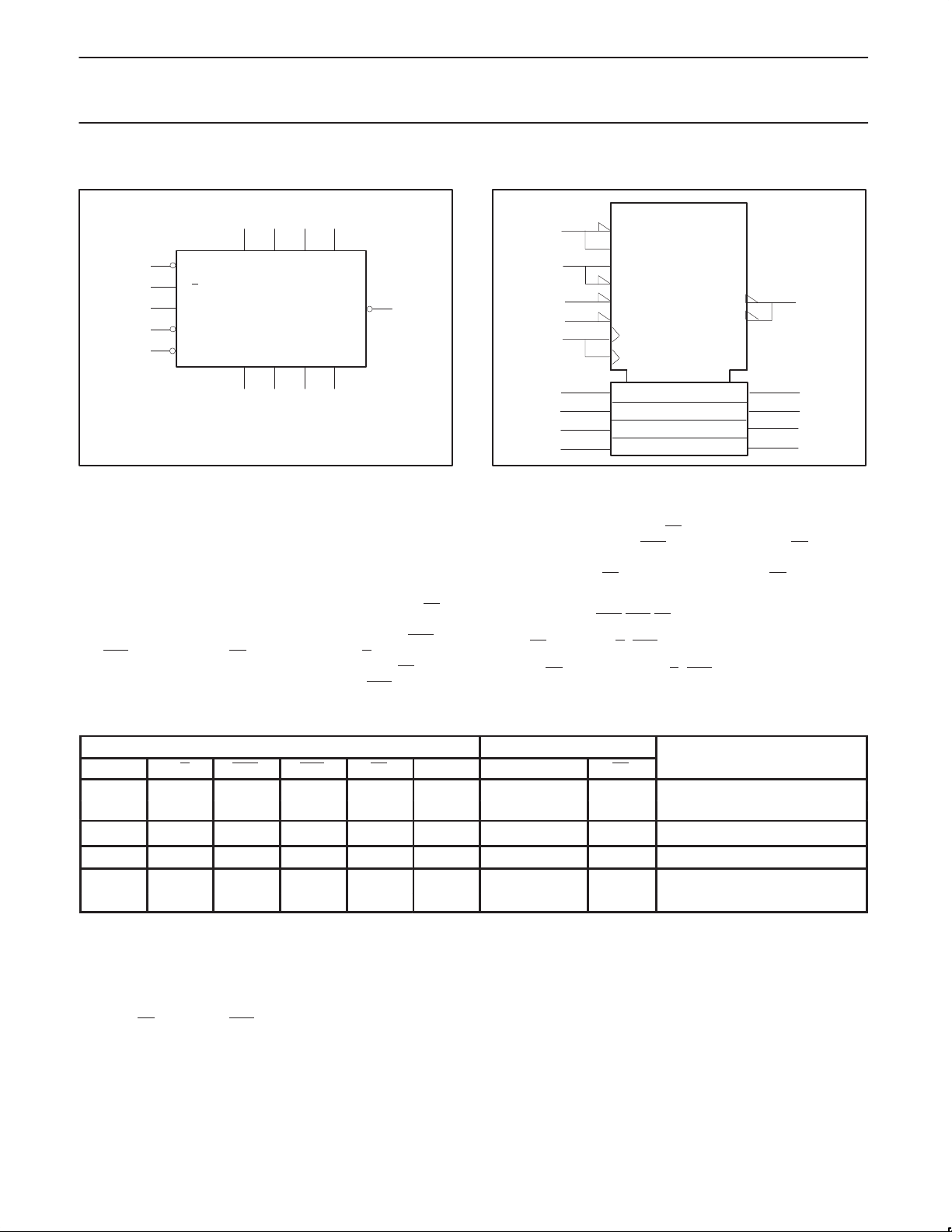
LOGIC SYMBOL
3456
D
0D1D2D3
Q0Q1Q2Q
TC
3
11121314
15
SF00786
10
VCC = Pin 16
GND = Pin 8
9
PE
1
U/D
CP
2
CEP
7
CET
FUNCTIONAL DESCRIPTION
The 74F169 uses edge-triggered J-K-type flip-flops and have no
constraints on changing the control or data input signals in either
state of the clock. The only requirement is that the various inputs
attain the desired state at least a setup time before the rising edge
of the clock and remain valid for the recommended hold time
thereafter. The parallel load operation takes precedence over the
other operations, as indicated in the Mode Select Table. When PE
Low, the data on the D
rising edge of the Clock. In order for counting to occur, both CEP
and CET must be Low and PE must be High; the U/D input
determines the direction of counting. The Terminal Count (TC
output is normally High and goes Low, provided that CET
- D3 inputs enter the flip-flops on the next
0
is Low,
)
LOGIC SYMBOL (IEEE/IEC)
9
1
10
7
2
3
4
5
6
when a counter reaches zero in the Count Down mode or reaches
15 in the Count Up mode. The TC
the Count Enable Parallel (CEP
derived by decoding the flip-flop states, there exists the possibility of
decoding spikes on TC
signal is not recommended (see logic equations below).
is
1) Count Enable = CEP⋅CET⋅PE
2) Up: TC = Q
3) Down: TC = Q
⋅(U/D)⋅CET
0⋅Q3
0⋅Q1⋅Q2⋅Q3
CTR DIV 16
M1 [LOAD]
M2 [COUNT]
M3 [UP]
M4 [DOWN]
G5
G6
2, 3, 5, 6+/C7
2, 4, 5, 6–
1, 7D
3, 5 CT=15
4, 5 CT=0
[1]
[2]
[4]
[8]
15
14
13
12
11
SF00787
output state is not a function of
) input level. Since the TC signal is
. For this reason the use of TC as a clock
⋅(U/D)⋅CET
MODE SELECT — FUNCTION TABLE
INPUTS OUTPUTS
CP U/D CEP CET PE D
n
↑ X X X l l L (1) Parallel load (Dn→Qn)
↑
↑
↑
↑
↑
X X X X X H (1)
h l l h X Count Up (1) Count Up (increment)
l l l h X Count Down (1) Count Down (decrement)
X h X h X q
X X X h X q
H = High voltage level steady state
h = High voltage level one setup time prior to the Low-to-High clock transition
L = Low voltage level steady state
l = Low voltage level one setup time prior to the Low-to-High clock transition
q = Lower case letters indicate the state of the referenced output prior to the Low-to-High clock transition
X = Don’t care
↑ = Low-to-High clock transition
(1)= The TC
is Low when CET is Low and the counter is at Terminal Count.
Terminal Count Up is (HHHH) and Terminal Count Down is (LLLL).
Q
n
n
n
TC
(1) Hold (do nothing)
H
1996 Jan 05
3
Philips Semiconductors Product specification
OPERATING MODE
74F1694-bit up/down binary synchronous counter
MODE SELECT TABLE
INPUTS
PE CEP CET U/D
L X X X Load(Dn→Qn)
H L L H Count Up (Increment)
H L L L Count Down (Decrement)
H H X X No Change (Hold)
H X H X No Change (Hold)
H = High Voltage
L = Low Voltage Level
X = Don’t care
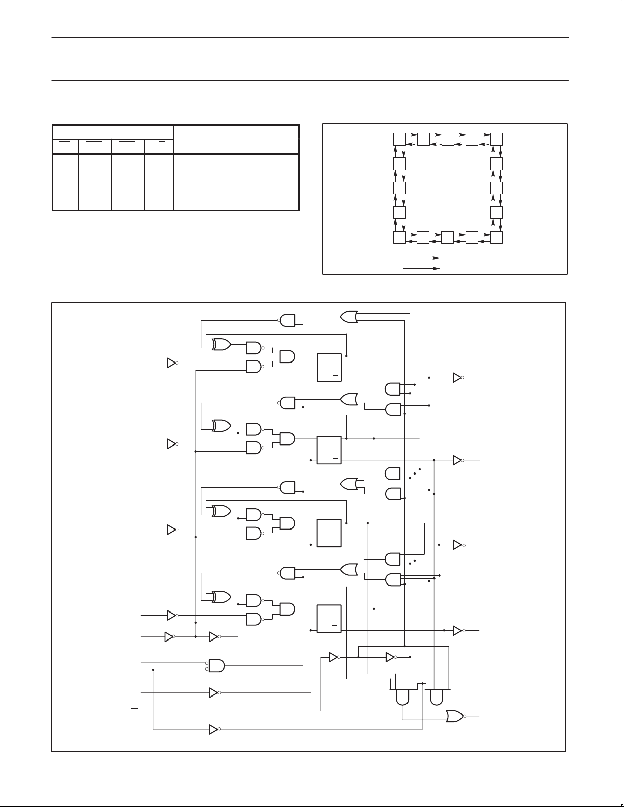
LOGIC DIAGRAM
3
D
0
STATE DIAGRAM
DCPQ
Q
01234
15
14
13
COUNT DOWN
COUNT UP
5
6
7
89101112
14
Q
0
SF00788
VCC= Pin 16
GND = Pin 8
PE
CEP
CET
CP
U/D
4
D
1
5
D
2
6
D
3
9
7
10
2
1
DCPQ
DCPQ
DCPQ
13
12
11
15
SF00789
Q
1
Q
2
Q
3
TC
Q
Q
Q
1996 Jan 05
4
 Loading...