Philips 74f151a DATASHEETS

INTEGRATED CIRCUITS
74F151A
8-input multiplexer
Product specification
Supercedes data of 1989 Mar 03
IC15 Data Handbook
1995 Jul 17

Philips Semiconductors Product specification
74F151A8-input multiplexer
FEA TURES
•High speed 8-to-1 multiplexing
•On chip decoding
•Multifunction capability
•Complementary outputs
DESCRIPTION
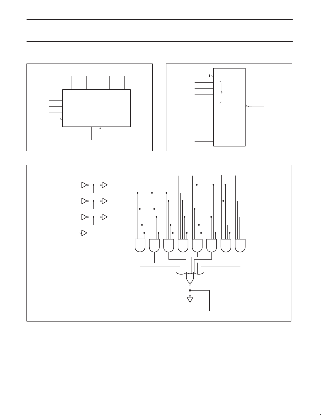
The 74F151A is a logic implementation of a single-pole, 8-position
switch with the switch position controlled by the state of three Select
(S0, S1, S2) inputs. True (Y) and complementary (Y
both provided. The Enable input (E
output is High and the Y output is Low, regardless of all other
the Y
) is active Low. When E is High,
inputs. In one package the 74F151A provides the ability to select
from eight sources of data or control information. The device can
provide any logic function of four variables and the negation with
correct manipulation.
) outputs are
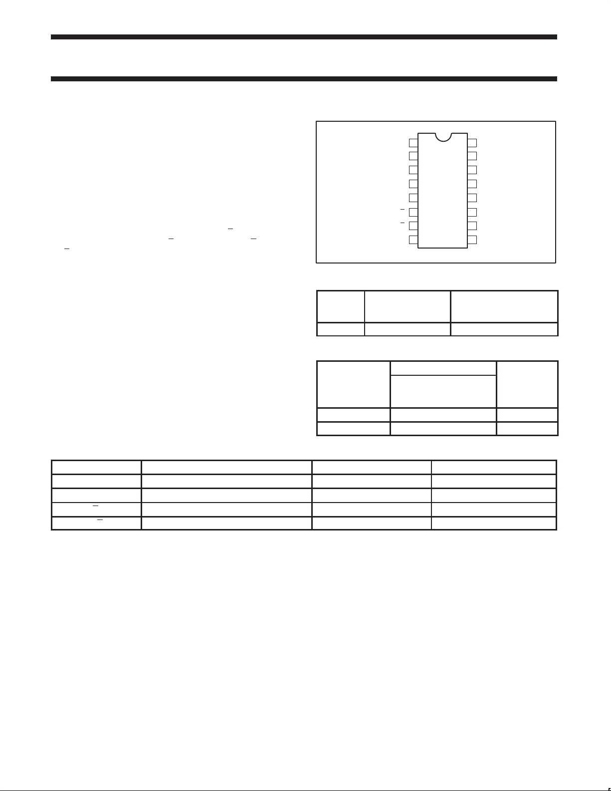
PIN CONFIGURATION
I3
1
I2
2
I1
3
I0
4
Y
5
Y
6
E
TYPICAL
TYPE
PROPAGATION
DELAY
74F151A 4.5ns 17mA
16
V
CC
I4
15
I5
14
I6
13
I7
12
S0
11
S1
107
98GND S2
SF00742
TYPICAL
SUPPLY CURRENT
(TOTAL)
ORDERING INFORMATION
ORDER CODE
DESCRIPTION
16-pin plastic DIP N74F151AN SOT38-4
16-pin plastic SO N74F151AD SOT109-1
COMMERCIAL RANGE
VCC = 5V ±10%,
T
= 0°C to +70°C
amb
PKG DWG #
INPUT AND OUTPUT LOADING AND FAN-OUT TABLE
PINS DESCRIPTION 74F (U.L.) HIGH/LOW LOAD VALUE HIGH/LOW
I0–I7 Data inputs 1.0/1.0 20µA/0.6mA
S0–S2 Select inputs 1.0/1.0 20µA/0.6mA
E Enable input (active High) 1.0/1.0 20µA/0.6mA
Y, Y Data outputs 150/33 3mA/20mA
NOTE:
One (1.0) FAST unit load is defined as: 20µA in the High state and 0.6mA in the Low state.
1995 Jul 17 853–1 158 15459
2

Philips Semiconductors Product specification
74F151A8-input multiplexer
LOGIC SYMBOL
11
10
9
7
VCC = Pin 16
GND = Pin 8
S0
S1
S2
E
LOGIC DIAGRAM
9
S2
10
S1
4 12131415
I0 I1 I2 I3 I4 I5 I6 I7
123
YY
65
SF00743
IEC/IEEE SYMBOL
7
11
10
9
4
3
2
1
15
14
13
12
I0 I1 I2 I3 I4 I5 I6 I7
4 3 2 1 15 14 13 12
EN
MUX
0
0
G
7
2
5
6
SF00744
V
= Pin 16
CC
GND = Pin 8
11
S0
7
E
56
YY
SF00741
1995 Jul 17
3
 Loading...