

Philips 74f1244 DATASHEETS

INTEGRATED CIRCUITS
74F1244
Octal buffer (3-State)
Product specification
IC15 Data Handbook
1989 Apr 04

Philips Semiconductors Product specification
74F1244Octal buffer (3-State)
FEA TURES
•High impedance NPN base inputs for reduced loading
(20µA in High and Low states)
•Low power, light loading
•Functional pin-for-pin equivalent of 74F244
•1/30th the bus loading of 74F244
•Provides ideal interface and increase fan-out of MOS
microprocessors
•Octal bus interface
•3-State buffer outputs sink 64mA and source 15mA
DESCRIPTION
The 74F1244 is an octal buffer that is ideal for driving bus lines or
buffer memory address registers. The outputs are capable of sinking
64mA and sourcing up to 15mA, producing very good capacitive
drive characteristics. The device features two Output Enables, OE
and OE
b, each controlling four of the 3-State outputs.
The 74F1244 is pin and functionally compatible with the 74F244.
The lower power and light bus loading features make it an ideal part
to interface directly with MOS microprocessors.
a
PIN CONFIGURATION
1
OEa
2
Ia0
3
Yb0
4
Ia1
5
Yb1
6
Ia2
7
Yb2
8
Ia3
9
Yb3
10 11
GND
TYPICAL
TYPE
PROPAGATION
DELAY
74F1244 4.5ns 43mA
20
V
CC
19
OEb
18
Ya0
17
Ib0
16
Ya1
15
Ib1
14
Ya2
13
Ib2
12
Ya3
Ib3
SF00227
TYPICAL SUPPL Y
CURRENT (TOTAL)
ORDERING INFORMATION
COMMERCIAL RANGE
V
DESCRIPTION
= 5V ±10%,
CC
T
= 0°C to +70°C
amb
20-pin plastic DIP N74F1244N SOT146-1
20-pin plastic SOL N74F1244D SOT163-1
DRAWING
NUMBER
INPUT AND OUTPUT LOADING AND FAN OUT TABLE
PINS DESCRIPTION
Ian, Ibn Data inputs 1.0/0.033 20µA/20µA
OEa, OEb Output enable inputs (active Low) 1.0/0.033 20µA/20µA
Yan, Ybn Data outputs 750/106.7 15mA/64mA
NOTE: One (1.0) FAST unit load is defined as: 20µA in the high state and 0.6mA in the low state.
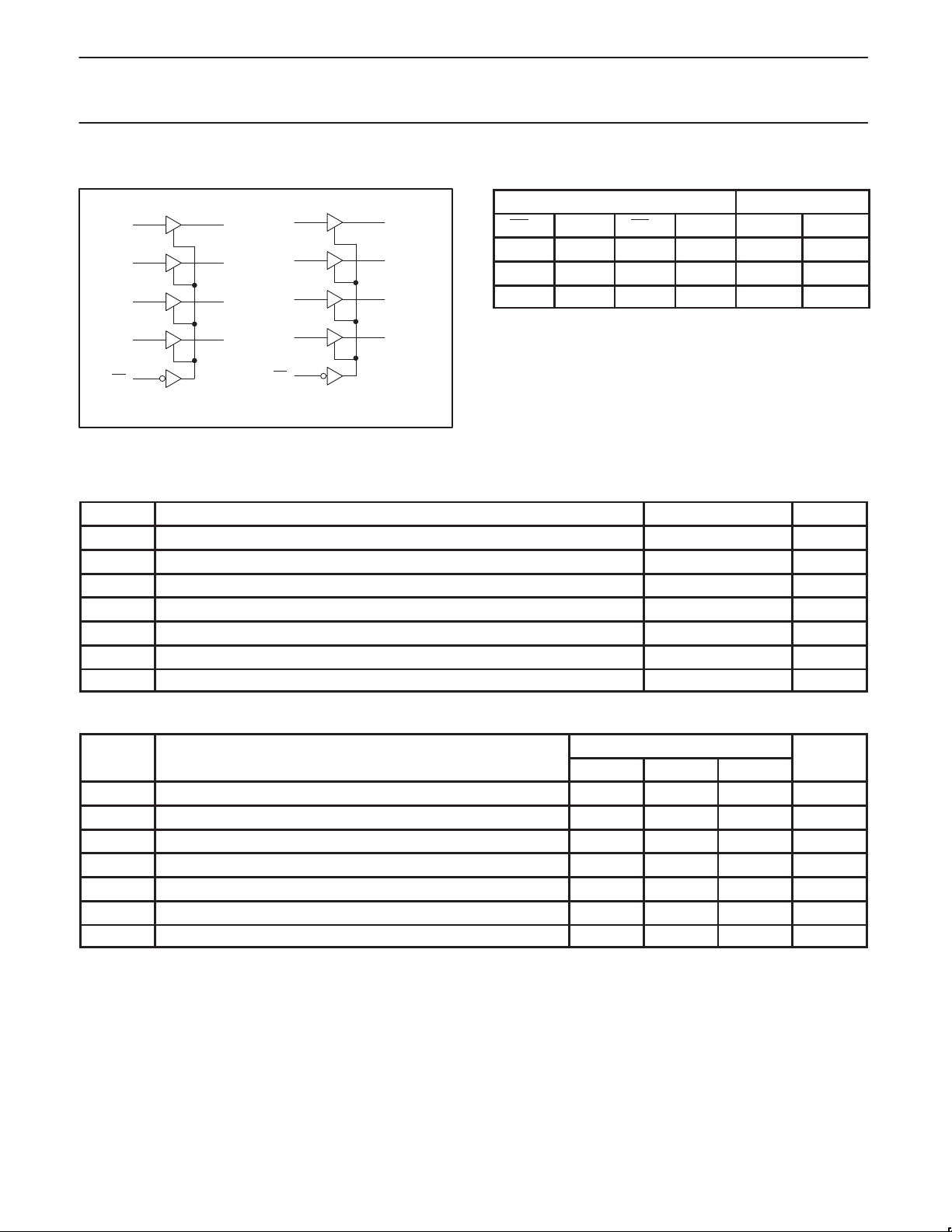
LOGIC SYMBOL
1
OEa
OEb19
V
= Pin 20
CC
GND = Pin 10
2 4 6 8 17 15 13 11
Ia0 Ia1 Ia2 Ia3 Ib0 Ib1 Ib2 Ib3
Ya0 Ya1 Ya2 Ya3 Yb0 Yb1 Yb2 Yb3
18 16 14 12 3 5 7 9
SF00228
IEC/IEEE SYMBOL
1
19
2
4
6
8
17
15
13
11
74F (U.L.)
HIGH/LOW
EN1
EN2
1
2
SF01366
LOAD VALUE
HIGH/LOW
18
16
14
12
3
5
7
9
1989 Apr 04 853–0041 96221
2
Philips Semiconductors Product specification
SYMBOL
PARAMETER
UNIT
74F1244Octal buffer (3-State)
LOGIC DIAGRAM
2
Ia0
4
Ia1
6
Ia2
18
Ya0
16
Ya1
14
Ya2
Ib0
Ib1
Ib2
17
15
13
3
Yb0
5
Yb1
7
Yb2
FUNCTION TABLE
OEa Ia OEb Ib Ya Yb
L L L L L L
L H L H H H
H X H X Z Z
H = High voltage level
Ia3
OEa
V
= Pin 20
CC
GND = Pin 10
8
1
12
Ya3
Ib3
OEb
11
19
9
SF00230
Yb3
L = Low voltage level
X = Don’t care
Z = High impedance “off” state
ABSOLUTE MAXIMUM RATINGS
(Operation beyond the limit set forth in this table may impair the useful life of the device.
Unless otherwise noted these limits are over the operating free-air temperature range.)
SYMBOL
V
CC
V
IN
I
IN
V
OUT
I
OUT
T
amb
T
stg
Supply voltage –0.5 to +7.0 V
Input voltage –0.5 to +7.0 V
Input current –30 to +5 mA
Voltage applied to output in High output state –0.5 to V
Current applied to output in Low output state 128 mA
Operating free-air temperature range 0 to +70 °C
Storage temperature range –65 to +150 °C
PARAMETER RATING UNIT
INPUTS OUTPUTS
CC
V
RECOMMENDED OPERATING CONDITIONS
V
V
V
I
I
I
T
CC
IH
IL
IK
OH
OL
amb
Supply voltage 4.5 5.0 5.5 V
High-level input voltage 2.0 V
Low-level input voltage 0.8 V
Input clamp current –18 mA
High-level output current –15 mA
Low-level output current 64 mA
Operating free-air temperature range 0 +70 °C
LIMITS
MIN NOM MAX
1989 Apr 04
3
 Loading...