

Philips 74F1240 Technical data
查询74F1240供应商
INTEGRATED CIRCUITS
74F1240
Octal inverter buffer (3-State)
74F1241
Octal buffer (3-State)*
* Discontinued part. Please see the Discontinued Product List.
Product specification
Supercedes data of 1989 Apr 04
IC15 Data Handbook
1999 Jan 08

Philips Semiconductors Product specification
74F1240, 74F1241*Buffers
74F1240 Octal inverter buffer (3-State)
FEATURES
•High impedance NPN base inputs for reduced loading
(20µA in High and Low states)
•Low power, light loading
•Functional pin-for-pin equivalent of 74F240 and 74F241
TYPE
74F1240 3.5ns 40mA
74F1241 4.5ns 46mA
TYPICAL
PROPAGATION
DELAY
•1/30th the bus loading of 74F240 and 74F241
•Provides ideal interface and increase fan-out of MOS
microprocessors
•Octal bus interface
•3-State buffer outputs sink 64mA
•15mA source current
DESCRIPTION
The 74F1240 and 74F1241 are octal buffers that are ideal for driving
bus lines or buffer memory address registers. The outputs are
capable of sinking 64mA and sourcing up to 15mA, producing very
good capacitive drive characteristics. The device features two
Output Enables, OE
outputs.
INPUT AND OUTPUT LOADING AND FAN OUT TABLE
PINS DESCRIPTION
Ian, Ibn Data inputs 1.0/0.033 20µA/20µA
OEa, OEb Output enable inputs (active Low) 1.0/0.033 20µA/20µA
OEb Output enable input (active High, 74F1241) 1.0/0.033 20µA/20µA
Yan, Ybn Data outputs (74F1241) 750/106.7 15mA/64mA
Yan, Ybn Data outputs (74F1240) 750/106.7 15mA/64mA
NOTE: One (1.0) FAST unit load is defined as: 20µA in the High state and 0.6mA in the Low state.
a and OEb, each controlling four of the 3-State
ORDERING INFORMATION
COMMERCIAL RANGE
V
DESCRIPTION
20-pin plastic DIP N74F1240N SOT146-1
20-pin plastic SOL N74F1240D SOT163-1
= 5V ±10%,
CC
T
= 0°C to +70°C
amb
74F (U.L.)
HIGH/LOW
TYPICAL
SUPPLY CURRENT
(TOTAL)
DRAWING
NUMBER
LOAD VALUE
HIGH/LOW
* Discontinued part. Please see the Discontinued Products List.
1999 Jan 08 853–0039 20619
2
Philips Semiconductors Product specification
74F1240, 74F1241*Buffers
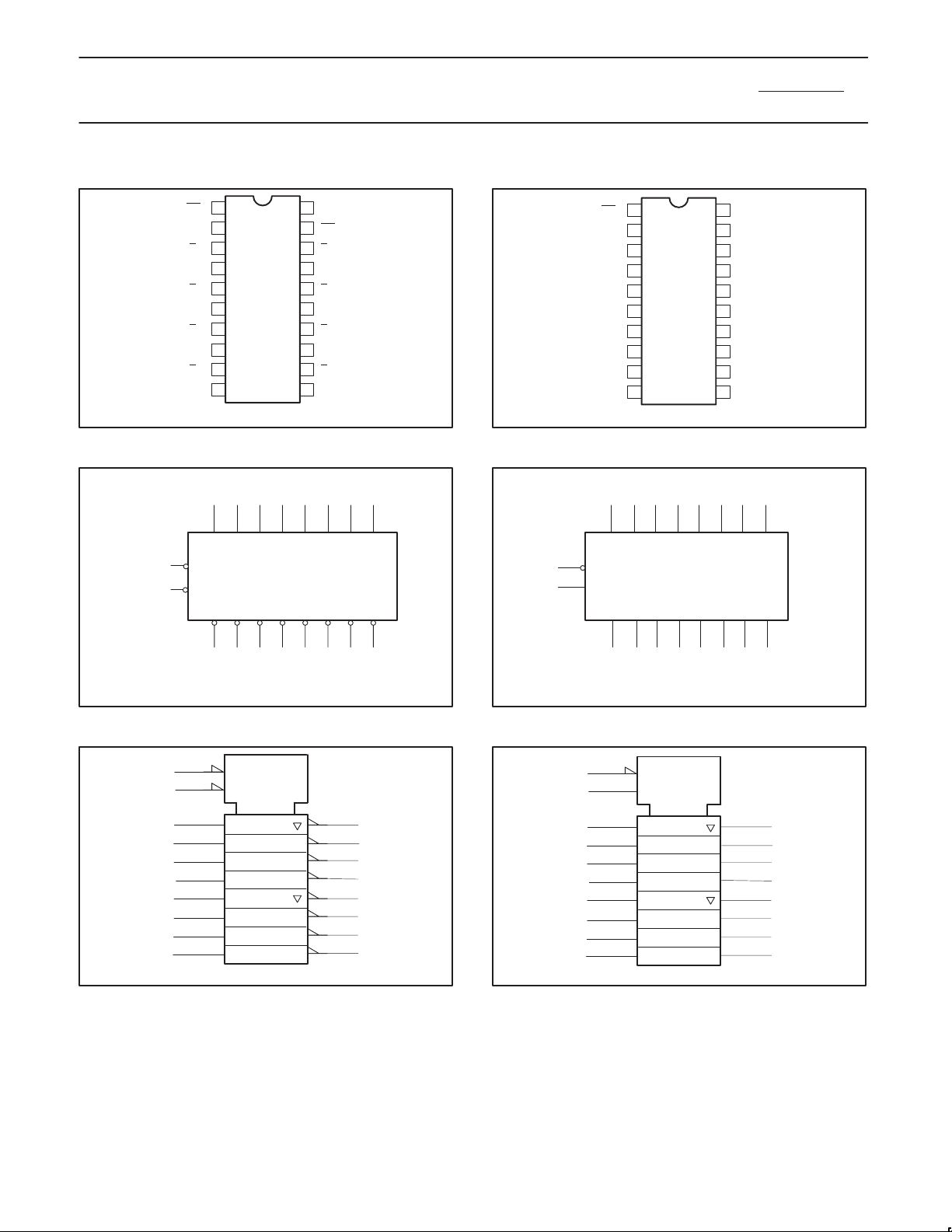
PIN CONFIGURATION – 74F1240
1
OEa
2
Ia0
3
Yb0
4
Ia1
5
Y
b1
6
Ia2
7
Y
b2
8
Ia3
9
Yb3
10 11
GND
20
19
18
17
16
15
14
13
12
SF00320
LOGIC SYMBOL – 74F1240
2 4 6 8 17 15 13 11
Ia0 Ia1 Ia2 Ia3 Ib0 Ib1 Ib2 Ib3
119OEa
OEb
Ya0 Ya1 Ya2 Ya3 Yb0 Yb1 Yb2 Yb3
V
OEb
Y
Ib0
Y
Ib1
Y
Ib2
Ya3
Ib3
PIN CONFIGURATION – 74F1241
V
1
CC
a0
a1
a2
OEa
2
Ia0
3
Yb0
4
Ia1
5
Yb1
6
Ia2
7
Yb2
8
Ia3
9
Yb3
10 11
GND
20
19
18
17
16
15
14
13
12
SF00324
CC
OEb
Ya0
Ib0
Ya1
Ib1
Ya2
Ib2
Ya3
Ib3
LOGIC SYMBOL – 74F1241
2 4 6 8 17 15 13 11
Ia0 Ia1 Ia2 Ia3 Ib0 Ib1 Ib2 Ib3
1
OEa
19
OEb
Ya0 Ya1 Ya2 Ya3 Yb0 Yb1 Yb2 Yb3
181614123579
VCC = Pin 20
GND = Pin 10
IEC/IEEE SYMBOL – 74F1240
1
19
2
4
6
8
17
15
13
11
EN1
EN2
18 16 14 12 3 5 7 9
VCC = Pin 20
SF00321
GND = Pin 10
SF00325
IEC/IEEE SYMBOL – 74F1241
1
19
1
2
18
16
14
12
3
5
7
9
SF01367
2
4
6
8
17
15
13
11
EN1
EN2
1
2
18
16
14
12
3
5
7
9
SF01368
* Discontinued part. Please see the Discontinued Products List.
1999 Jan 08
3
 Loading...