

Philips 74f113 DATASHEETS
INTEGRATED CIRCUITS
74F113
Dual J-K negative edge-triggered
flip-flops without reset
Product specification
IC15 Data Handbook
1991 Feb 14

Philips Semiconductors Product specification
Dual J-K negative edge-triggered flip-flops
without reset
FEA TURE
•Industrial temperature range available (–40°C to +85°C)
DESCRIPTION
The 74F113, dual negative edge-triggered JK-type flip-flop, features
individual J, K, clock (CP
outputs. The asynchronous S
to the steady state levels as shown in the function table regardless
of the level at the other inputs.
A high level on the clock (CP
data will be accepted. The logic levels at the J and K inputs may be
allowed to change while the CP
according to the function table as long as minimum setup and hold
times are observed. Output changes are initiated by the high-to-low
transition of the CP
TYPE TYPICAL f
74F113 100MHz 15mA
ORDERING INFORMATION
DESCRIPTION
14-pin plastic DIP N74F113N I74F1 13N SOT27–1
14-pin plastic SO N74F113D I74F1 13D SOT108–1
), set (SD) inputs, true and complementary
D input, when low, forces the outputs
) input enables the J and K inputs and
is high and flip-flop will perform
.
COMMERCIAL RANGE
VCC = 5V ±10%,
T
= 0°C to +70°C
amb
max
ORDER CODE
PIN CONFIGURATION
CP
1
0
2
K0
J0
3
S
D0
4
Q0
5
0
6
Q
GND
TYPICAL SUPPLY CURRENT (TOTAL)
INDUSTRIAL RANGE
VCC = 5V ±10%,
T
= –40°C to +85°C
amb
14
13
12
11
10
9
87
SF00140
V
CP
K1
J1
SD1
Q1
Q1
74F1 13
CC
1
PKG. DWG. #
INPUT AND OUTPUT LOADING AND FAN-OUT TABLE
PINS DESCRIPTION 74F (U.L.) HIGH/LOW LOAD VALUE HIGH/LOW
J0, J1 J inputs 1.0/1.0 20µA/0.6mA
K0, K1 K inputs 1.0/1.0 20µA/0.6mA
CP0, CP1 Clock inputs (active falling edge) 1.0/4.0 20µA/2.4mA
SD0, SD1 Set inputs (active low) 1.0/5.0 20µA/3.0mA
Q0, Q1, Q0, Q1 Data outputs 50/33 1.0mA/20mA
NOTE:
One (1.0) FAST unit load is defined as: 20µA in the High state and 0.6mA in the Low state.
LOGIC SYMBOL
1
4
13
10
VCC = Pin 14
GND = Pin 7
CP0
SD0
CP1
SD1
311
J1 K0
Q0 Q0
56
212
K1J0
Q1 Q1
98
SF00141
IEC/IEEE SYMBOL
3
1
2
4
11
13
12
10
1J
C1
1K
1S
2J
C2
2K
2S
5
6
9
8
SF00142
1996 Mar 14 853–0339 16575
2
Philips Semiconductors Product specification
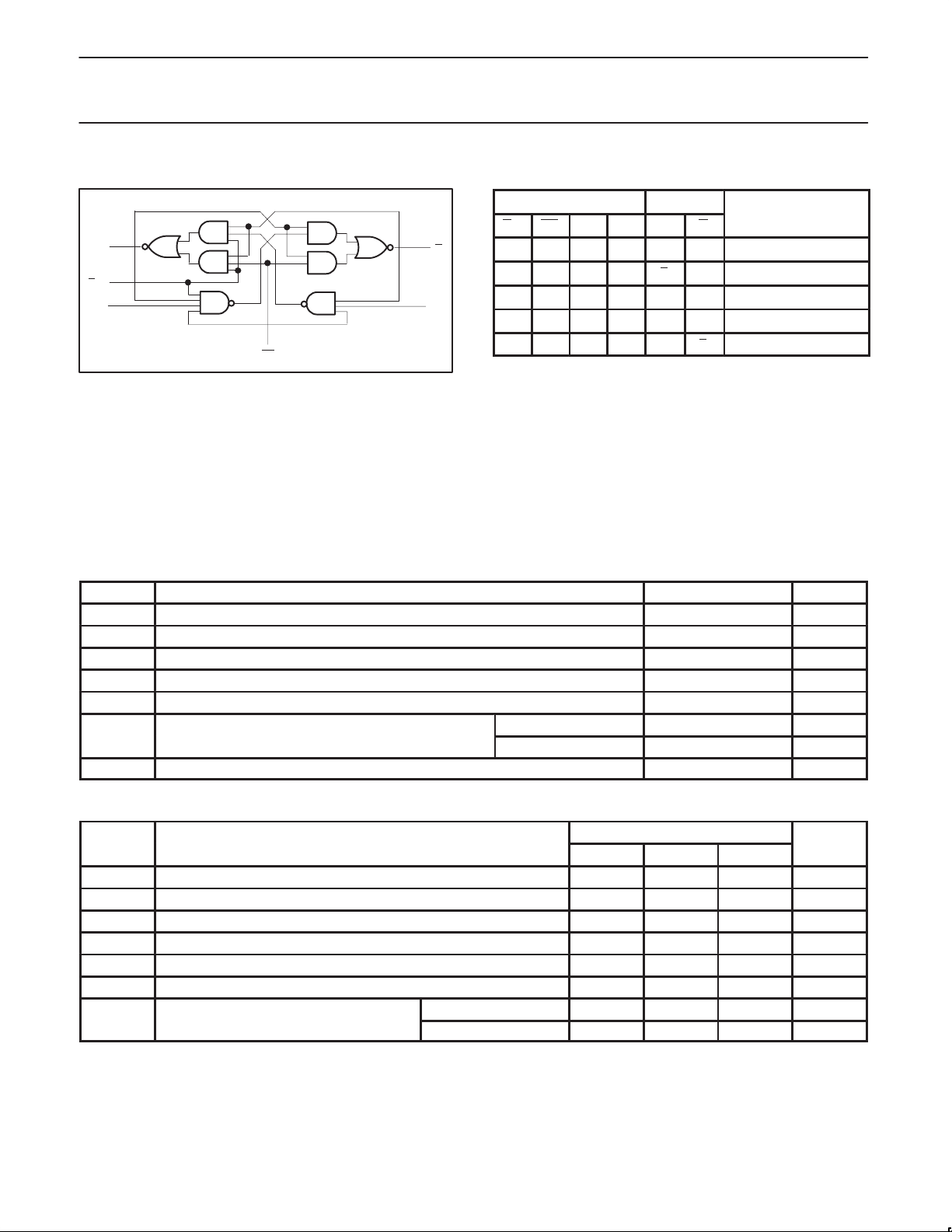
OPERATING MODE
T
Operating free-air temperature range
SYMBOL
PARAMETER
UNIT
T
Operating free-air temperature range
Dual J-K negative edge-triggered flip-flops
without reset
LOGIC DIAGRAM
5, 9
Q
4, 10
S
D
2, 12
K
V
= Pin 14
CC
GND = Pin 7
1, 13
CP
6, 8
3, 11
SF00143
Q
J
74F113
FUNCTION TABLE
INPUTS OUTPUTS
SD CP J K Q Q
L X X X H L Asynchronous set
H ↓ h h q q Toggle
H ↓ h l H L Load ”1” (set)
H ↓ l h L H Load ”0” (reset)
H ↓ l l q q Hold ’no change”
NOTES:
H = High-voltage level
h = High-voltage level one setup time prior to high-to-low
clock transition
L = Low-voltage level
l = Low-voltage level one setup time prior to high-to-low clock
transition
q = Lower case indicate the state of the referenced output
prior to the high-to-low clock transition
X = Don’t care
↓ = high-to-low clock transition
ABSOLUTE MAXIMUM RATINGS
(Operation beyond the limits set forth in this table may impair the useful life of the device.
Unless otherwise noted these limits are over the operating free-air temperature range.)
SYMBOL
V
CC
V
IN
I
IN
V
OUT
I
OUT
amb
T
stg
Supply voltage –0.5 to +7.0 V
Input voltage –0.5 to +7.0 V
Input current –30 to +5 mA
Voltage applied to output in High output state –0.5 to V
Current applied to output in Low output state 40 mA
p
p
Storage temperature range –65 to +150 °C
PARAMETER RATING UNIT
Commercial range 0 to +70 °C
Industrial range –40 to +85 °C
RECOMMENDED OPERATING CONDITIONS
V
V
V
I
I
I
CC
IH
IL
IK
OH
OL
amb
Supply voltage 4.5 5.0 5.5 V
High-level input voltage 2.0 V
Low-level input voltage 0.8 V
Input clamp current –18 mA
High-level output current –1 mA
Low-level output current 20 mA
p
p
Commercial range 0 +70 °C
Industrial range –40 +85 °C
CC
LIMITS
MIN NOM MAX
V
1996 Mar 14
3
 Loading...