

Philips 74AVC16834 Datasheet
INTEGRATED CIRCUITS
74AVC16834
18-bit registered driver
with inverted register enable (3-State)
Preliminary specification
Replaces datasheet 74AVC16834/74AVCH16834 dated 1998 Dec 11
1999 Jul 23
Philips Semiconductors Preliminary specification
1
CPDPower dissi ation ca acitance er buffer
V
GND to V
1
F
18-bit registered driver with inverted register enable
(3-State)
FEATURES
•Wide supply voltage range of 1.2 V to 3.6 V
•Complies with JEDEC standard no. 8-1A/5/7.
•CMOS low power consumption
•Input/output tolerant up to 3.6 V
•DCO (Dynamic Controlled Output) circuit dynamically changes
output impedance, resulting in noise reduction without speed
degradation
•Low inductance multiple V
and GND pins for minimum noise
CC
and ground bounce
•Power off disables 74AVC16834 outputs, permitting Live Insertion
DESCRIPTION
The 74AVC16834 is a 18-bit universal bus driver. Data flow is
controlled by output enable (OE
(CP).
This product is designed to have an extremely fast propagation
delay and a minimum amount of power consumption.
To ensure the high-impedance state during power up or power
down, OE
should be tied to VCC through a pullup resistor (Live
Insertion).
A Dynamic Controlled Output (DCO) circuitry is implemented to
support termination line drive during transient. See the graphs on
page 8 for typical curves.
), latch enable (LE) and clock inputs
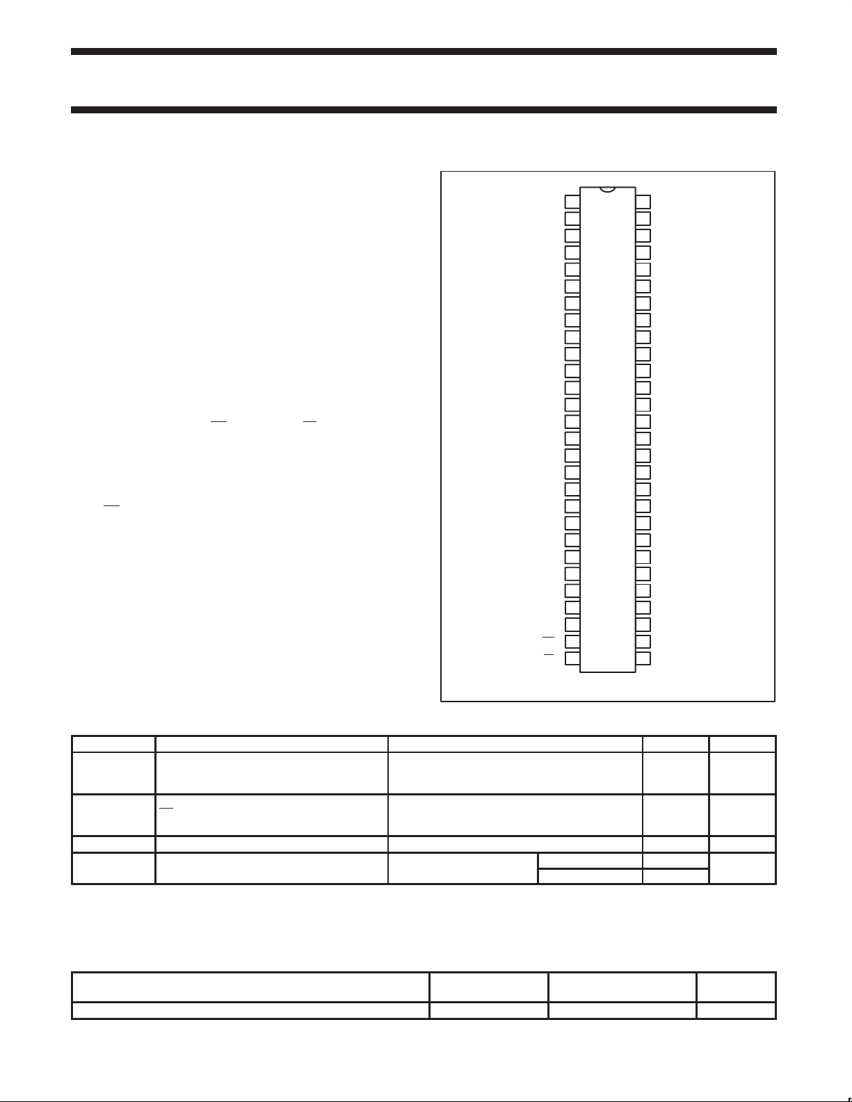
PIN CONFIGURATION
1
2
NC
3
Y
0
4
GND
5
Y
1
Y
6
2
V
7
CC
Y
8
3
Y
9
4
10
Y
5
11
GND
12
Y
6
13
Y
7
14
Y
8
15
Y
9
16
Y
10
17
Y
11
18
GND
19
Y
12
20
Y
13
21
Y
14
22
V
CC
23
Y
15
24
Y
16
25
GND
26
Y
17
27
OE
28 29
LE
74A VC16834
56NC
GND
55
NC
54
A
0
53
GND
52
A
1
A
51
2
V
50
CC
A
49
3
A
48
4
47
A
5
46
GND
45
A
6
44
A
7
43
A
8
42
A
9
41
A
10
40
A
11
39
GND
38
A
12
37
A
13
36
A
14
35
V
CC
34
A
15
33
A
16
32
GND
31
A
17
30
CP
GND
QUICK REFERENCE DA TA
GND = 0 V; T
SYMBOL
t
PHL/tPLH
t
PHL/tPLH
C
I
NOTES:
is used to determine the dynamic power dissipation (PD in µW):
1. C
PD
= CPD × V
P
D
= output frequency in MHz; VCC = supply voltage in V; S (CL × V
f
o
= 25°C; tr = tf ≤ 2.0 ns; CL = 30 pF.
amb
Propagation delay
An to Yn
Propagation delay
LE to Yn;
CP to Yn
Input capacitance 5.0 pF
2
× fi + S (CL × V
CC
ORDERING INFORMATION
56-Pin Plastic Thin Shrink Small Outline (TSSOP) Type II –40°C to +85°C 74AVC16834 DGG SOT364-1
1999 Jul 23
SH00156
PARAMETER CONDITIONS TYPICAL UNIT
p
CC
p
2
PACKAGES
VCC = 1.8 V
VCC = 2.5 V
VCC = 3.3 V
VCC = 1.8 V
VCC = 2.5 V
VCC = 3.3 V
p
× fo) where: fi = input frequency in MHz; CL = output load capacitance in pF;
=
I
CC
CC
2
× fo) = sum of outputs.
TEMPERATURE
RANGE
Outputs enabled 25
Output disabled 6
ORDER CODE
2.6
2.0
1.7
2.9
2.3
1.9
2
ns
ns
p
DRAWING
NUMBER
Philips Semiconductors Preliminary specification
OUTPUTS
18-bit registered driver with inverted register enable
(3-State)
PIN DESCRIPTION
PIN NUMBER SYMBOL NAME AND FUNCTION
1, 2, 55 NC No connection
3, 5, 6, 8, 9, 10, 12, 13,
14, 15, 16, 17, 19, 20,
Y0 to Y17Data outputs
21, 23, 24, 26
4, 11, 18, 25, 32, 39, 46,
53, 56
7, 22, 35, 50 V
27 OE
28 LE
GND Ground (0 V)
Positive supply voltage
CC
Output enable input
(active LOW)
Latch enable input
(active LOW)
30 CP Clock input
54, 52, 51, 49, 48, 47,
45, 44, 43, 42, 41, 40,
A0 to A17Data inputs
38, 37, 36, 34, 33, 31
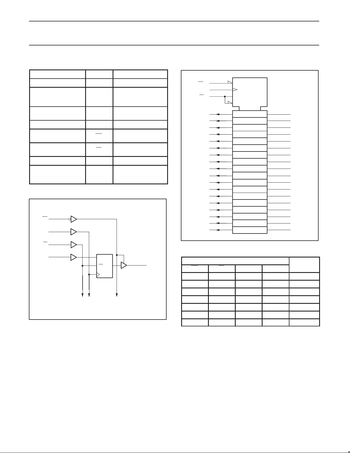
LOGIC SYMBOL
OE
CP
LE
A
0
TO THE 17 OTHER CHANNELS
D
LE
CP
Y
SH00157
0
LOGIC SYMBOL (IEEE/IEC)
OE
CP
LE
Y
Y
Y
Y
Y
Y
Y
Y
Y
Y
Y
10
Y
11
Y
12
Y
13
Y
14
Y
15
Y
16
Y
17
FUNCTION TABLE
OE LE CP A
H X X X Z
L L X L L
L L X H H
L H ↑ L L
L H ↑ H H
L H H X Y
L H L X Y
H = HIGH voltage level
L = LOW voltage level
X = Don’t care
Z = High impedance “off” state
↑ = LOW-to-HIGH level transition
NOTES:
1. Output level before the indicated steady-state input conditions
were established, provided that CP is high before LE goes low.
2. Output level before the indicated steady-state input conditions
were established.
74A VC16834
27
30
28
3
0
5
1
6
2
8
3
9
4
10
5
12
6
13
7
14
8
15
9
16
17
19
20
21
23
24
26
EN1
C3
G2
1 ∇ 1
INPUTS
2C3
54
A
0
52
A
1
51
A
2
3D
49
A
3
48
A
4
47
A
5
45
A
6
44
A
7
43
A
8
42
A
9
41
A
10
40
A
11
38
A
12
37
A
13
36
A
14
34
A
15
33
A
16
31
A
17
SH00158
1
0
2
0
1999 Jul 23
3
 Loading...