

Philips 74AVC16373 Datasheet

INTEGRATED CIRCUITS
DATA SH EET
74AVC16373
16-bit D-type transparent latch;
3.6 V tolerant; 3-state
Product Specification
Supersedes data of 1998 Dec 11
File under Integrated Circuits, IC24
2000 Mar 09
Philips Semiconductors Product Specification
16-bit D-type transparent latch; 3.6 V tolerant;
3-state
FEATURES
• Wide supply voltage range from 1.2 to 3.6 V
• Complies with JEDEC standard no. 8-1A/5/7
• CMOS low power consumption
• Input/output tolerant up to 3.6 V
• Dynamic Controlled Output (DCO) circuit dynamically
changes output impedance,resulting in noise reduction
without speed degradation
• Low inductance multiple VCCand GND pins to minimize
noise and ground bounce
• Supports Live Insertion.
DESCRIPTION
The 74AVC16373 is a 16-bit D-type transparent latch
featuring separate D-type inputs for each latch, and
3-state outputs for bus oriented applications. One Latch
Enable (LE) input and one Output Enable (OE) input are
provided per 8-bit section. The 74AVC16373 consist of
two sections of eight D-type transparent latches with
3-state true outputs.
The 74AVC16373 is designed to have an extremely fast
propagation delay and a minimum amount of power
consumption.
To ensure the high-impedance output state during
power-up or power-down, pin OEn should be tied to V
through a pull-up resistor (Live Insertion).
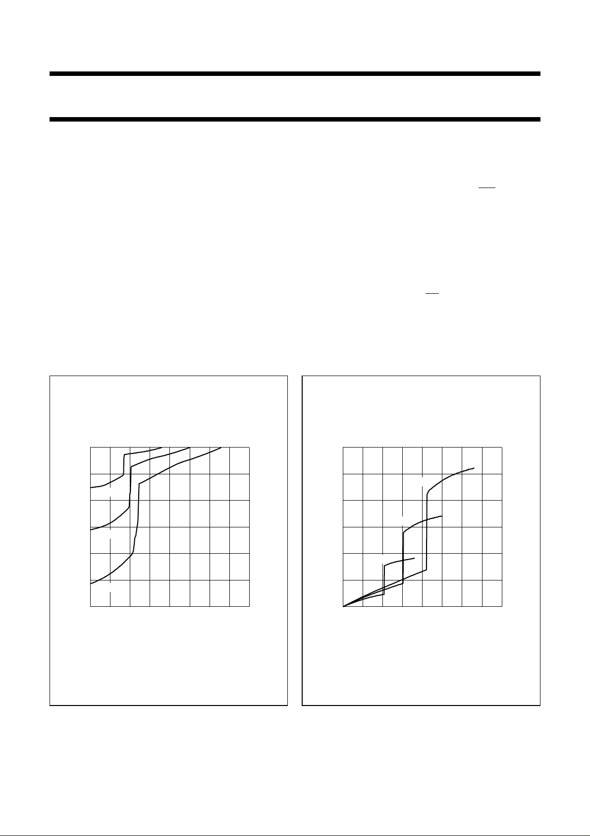
A Dynamic Controlled Output (DCO) circuitry is
implemented to support termination line drive during
transient (see Figs 1 and 2).
74AVC16373
CC
handbook, halfpage
0
I
OH
(mA)
1.8 V
−100
2.5 V
−200
3.3 V
−300
012 4
Fig.1 Output voltage as a function of the
HIGH-level output current.
3
VOH (V)
MNA506
300
handbook, halfpage
I
OL
(mA)
200
100
0
012 4
1.8 V
3.3 V
2.5 V
Fig.2 Output voltage as a function of the
LOW-level output current.
3
MNA507
VOL (V)
2000 Mar 09 2

Philips Semiconductors Product Specification
16-bit D-type transparent latch; 3.6 V tolerant;
3-state
QUICK REFERENCE DATA
GND = 0 V; T
t
PHL/tPLH
C
I
C
PD
Notes
1. C
is used to determine the dynamic power dissipation (PDin µW).
PD
PD=CPD× V
fi= input frequency in MHz;
fo= output frequency in MHz;
CL= output load capacitance in pF;
VCC= supply voltage in Volts;
∑ (CL× V
2. The condition is VI= GND to VCC.
=25°C; tr=tf≤2.0 ns.
amb
SYMBOL PARAMETER CONDITIONS TYP. UNIT
propagation delay
nDnto nQ
n
input capacitance 5.0 pF
power dissipation
capacitance per buffer
2
× fi+ ∑ (CL× V
CC
2
× fo) = sum of outputs.
CC
2
× fo) where:
CC
74AVC16373
VCC= 1.2 V 3.6 ns
V
= 1.5 V 3.1 ns
CC
V
= 1.8 V 2.2 ns
CC
= 2.5 V 1.6 ns
V
CC
V
= 3.3 V 1.4 ns
CC
notes 1 and 2
outputs enabled 34 pF
outputs disabled 1 pF
FUNCTION TABLE
See note 1.
OPERATING MODES
n
Enable and read register
(transparent mode)
Latch and read register
(hold mode)
Latch register and disable outputs H
INPUTS
OE LE nA
L
L
L
L
H
H
L
L
L
H
L
n
L
H
l
h
l
h
INTERNAL
LATCHES
Note
1. H = HIGH voltage level;
h = HIGH voltage level one set-up time prior to the HIGH-to-LOW LE transition;
L = LOW voltage level;
l = LOW voltage level one set-up time prior to the HIGH-to-LOW LE transition;
Z = high impedance OFF-state.
OUTPUTS
nY
n
L
H
L
H
L
H
L
H
L
H
Z
Z
2000 Mar 09 3
Philips Semiconductors Product Specification
16-bit D-type transparent latch; 3.6 V tolerant;
74AVC16373
3-state
ORDERING AND PACKAGE INFORMATION
to 1Q
to 2Q
to 2D
to 1D
PACKAGE
data outputs
7
DC supply voltage
data outputs
7
data inputs
0
data inputs
0
TYPE NUMBER
TEMPERATURE RANGE PINS PACKAGE MATERIAL CODE
74AVC16373DGG −40 to +85 °C 48 TSSOP plastic SOT362-1
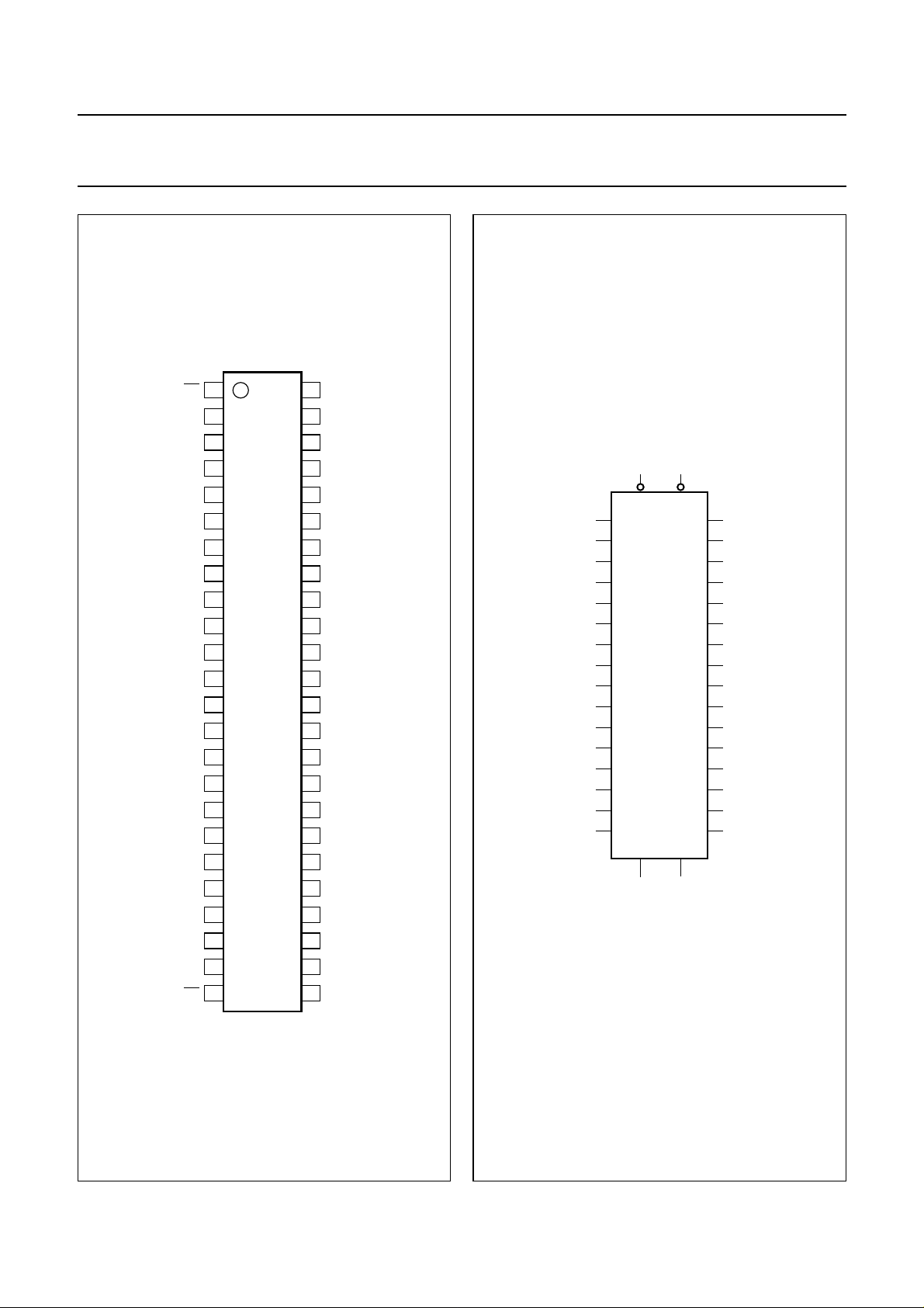
PINNING
PIN SYMBOL DESCRIPTION
11
2, 3, 5, 6, 8, 9, 11 and 12 1Q
OE output enable input (active LOW)
0
4, 10, 15, 21, 28, 34, 39 and 45 GND ground (0 V)
7, 18, 31 and 42 V
13, 14, 16, 17, 19, 20, 22 and 23 2Q
24 2
CC
0
OE output enable input (active LOW)
25 2LE latch enable input (active HIGH)
26, 27, 29, 30, 32, 33, 35 and 36 2D
37, 38, 40, 41, 43, 44, 46 and 47 1D
7
7
48 1LE latch enable input (active HIGH)
2000 Mar 09 4
Philips Semiconductors Product Specification
16-bit D-type transparent latch; 3.6 V tolerant;
3-state
handbook, halfpage
1OE
1Q
1Q
GND
1Q
1Q
V
CC
1Q
1Q
GND
1Q
1Q
2Q
2Q
GND
2Q
2Q
V
CC
2Q
2Q
GND
2Q
2Q
2OE
1
2
0
3
1
4
5
2
6
3
7
8
4
9
5
10
11
6
12
7
0
1
2
3
4
5
6
7
16373
13
14
15
16
17
18
19
20
21
22
23
24
MNA541
1LE
48
1D
47
0
1D
46
1
GND
45
1D
44
2
1D
43
3
V
42
CC
1D
41
4
1D
40
5
GND
39
1D
38
6
1D
37
7
2D
36
0
2D
35
1
GND
34
2D
33
2
2D
32
3
V
31
CC
2D
30
4
2D
29
5
GND
28
2D
27
6
2D
26
7
2LE
25
handbook, halfpage
74AVC16373
1
24
1OE
2OE
47
1D
0
46
1D
1
1D
44
43
41
40
38
37
36
35
33
32
30
29
27
26
2
1D
3
1D
4
1D
5
1D
6
1D
7
2D
0
2D
1
2D
2
2D
3
2D
4
2D
5
2D
6
2D
7
1LE 2LE
48 25
1Q
1Q
1Q
1Q
1Q
1Q
1Q
1Q
2Q
2Q
2Q
2Q
2Q
2Q
2Q
2Q
0
1
2
3
4
5
6
7
0
1
2
3
4
5
6
7
MNA547
2
3
5
6
8
9
11
12
13
14
16
17
19
20
22
23
Fig.3 Pin configuration.
2000 Mar 09 5
Fig.4 Logic symbol.
 Loading...