

Philips 74AVC16245DGG, 74AVCH16245DGG Datasheet

DATA SH EET
Objective specification
File under Integrated Circuits, IC24
1998 Dec 11
INTEGRATED CIRCUITS
74AVC16245; 74AVCH16245
16-bit transceiver with direction pin;
3-state
1998 Dec 11 2
Philips Semiconductors Objective specification
16-bit transceiver with direction pin; 3-state
74AVC16245;
74AVCH16245
FEATURES
• Wide supply voltage range of 1.2 V to
3.6 V
• Complies with JEDEC standard
no. 8-1A/5/7
• CMOS low power consumption
• Input/Output tolerant up to 3.6 V
• DCO (Dynamic Controlled Output) Circuit
dynamically changes output impedance,
resulting innoise reduction without speed
degradation
• Low inductance multiple VCC and GND
pins for minimize noise and ground
bounce.
• All data inputs have bushold.
(only 74AVCH16245)
• Power off disables 74AVC16245;
74AVCH16245 outputs, permitting Live
Insertion.
DESCRIPTION
The 74AVC(H)16245 is a 16-bit transceiver
featuring non-inverting 3-state bus compatible
outputs in both send and receive directions.
The AVCH16245 features two output enable
(nOE) inputs for easy cascading and two
send/receive (nDIR) inputsfor direction control.
nOE controls the outputs so that the buses are
effectively isolated. This device canbe used as
two 8-bit transceivers or one 16-bit transceiver.
This product is designed to have an extremely
fast propagation delay and a minimum amount
of power consumption.
To ensure the high-impedance output state
during powerup or power down,OEnshould be
tied to VCC through a pullup resistor (Live
insertion).
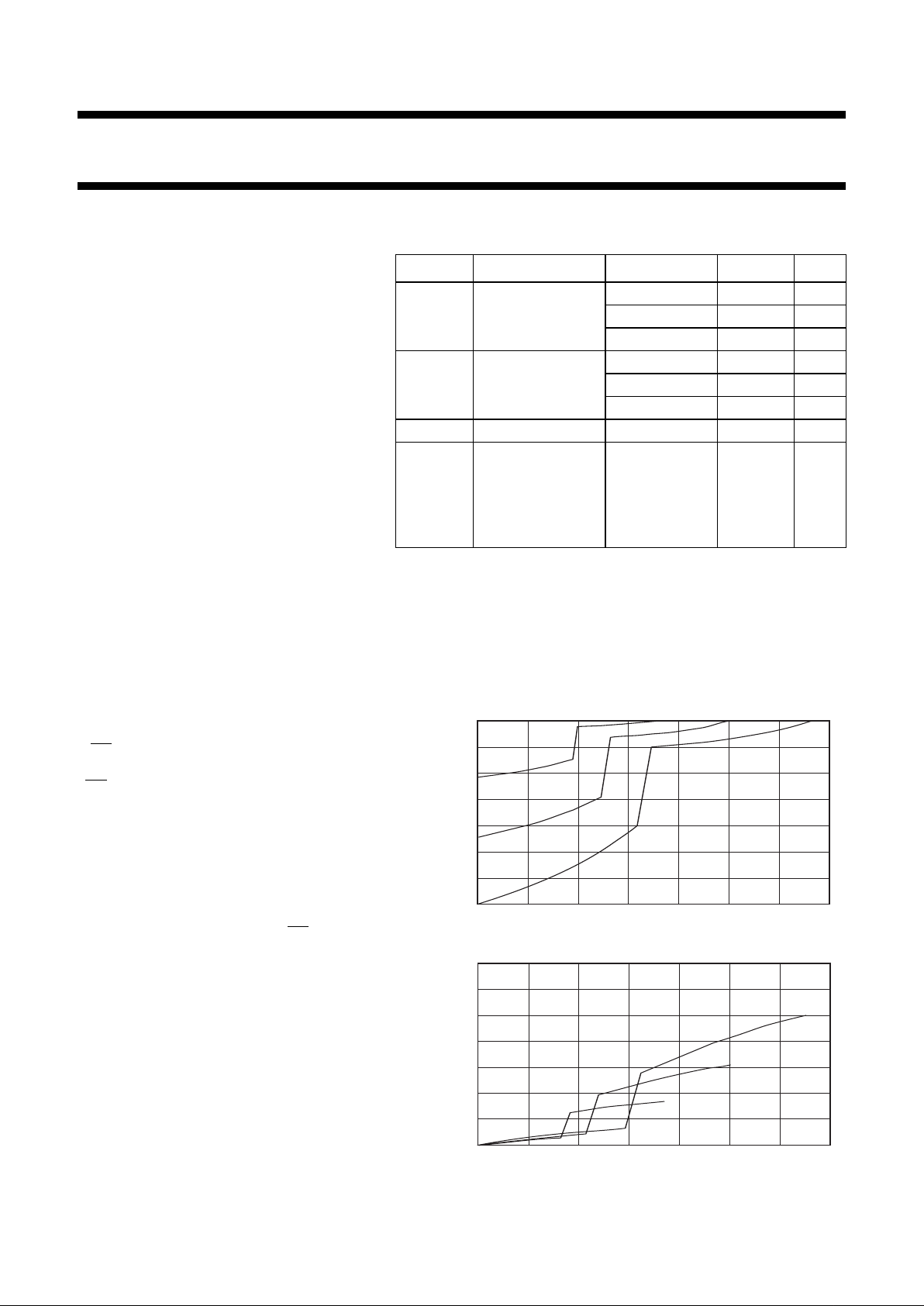
A Dynamic Controlled Output(DCO) circuitry is
implemented to support termination line drive
during transient. See graphs at this page for
typical curves.
The 74AVCH16245has active bushold circuitry
whichis providedto holdunused orfloatingdata
inputs at a valid logic level. This feature
eliminates the need for external pull-up or
pull-down resistors.
QUICK REFERENCE DATA
GND = 0 V; T
amb
=25°C; tr=tf≤2.0 ns; CL=30pF.
Notes
1.
CPDis used to determine the dynamic power dissipation (PDin µW).
P
D
= CPD× V
CC
2
× fi+ ∑ (CL× V
CC
2
× fo) where:
f
i
= input frequency in MHz;
f
o
= output frequency in MHz;
C
L
= output load capacitance in pF;
V
CC
= supply voltage in V;
∑ (C
L
× V
CC
2
× fo) = sum of outputs.
2. The condition is V
I
= GND to V
CC.
3. For type with bushold
SYMBOL PARAMETER CONDITIONS TYPICAL UNIT
t
PHL
/ t
PLH
propagation delay
An to Y
n
VCC= 1.8 V 1.5 ns
V
CC
= 2.5 V 1.1 ns
V
CC
= 3.3 V 1.0 ns
t
PHL
/ t
PLH
propagation delay
A
n
to Y
n
VCC= 1.8 V
(3)
1.5 ns
V
CC
= 2.5 V
(3)
1.1 ns
V
CC
= 3.3 V
(3)
1.0 ns
C
I
input capacitance 5.0 pF
C
PD
power dissipation
capacitance per
buffer
notes 1 and 2
outputs
enabled
20 pF
output
disabled
4pF
0
VOH(V) OUTPUT VOLTAGE
0
1.0 2.0 3.0
0.5 1.5
2.5
3.5
-300
-350
-200
-250
-150
-50
-100
I
OH
(V) OUTPUT CURRENT
PMOS
3.3V
2.5V
1.8V
0
VOL(V) OUTPUT VOLTAGE
1.0 2.0 3.00.5 1.5
2.5
3.5
0
-300
-200
-250
-150
-50
-100
I
OL
(V) OUTPUT CURRENT
NMOS
1.8V
3.3V
2.5V
-350

1998 Dec 11 3
Philips Semiconductors Objective specification
16-bit transceiver with direction pin; 3-state
74AVC16245;
74AVCH16245
FUNCTION TABLE
See Note 1.
Note
1. H - HIGH voltage level;
L - LOW voltage level;
X- don’t care;
Z - high impedance OFF-state.
ORDERING AND PACKAGE INFORMATION
PINNING
INPUTS INPUTS/OUTPUTS
n
OE nDIR nA
n
nB
n
L L A = B inputs
L H inputs B = A
HX Z Z
OUTSIDE NORTH
AMERICA
NORTH
AMERICA
PACKAGES
TEMPERATURE
RANGE
PINS PACKAGE MATERIAL CODE
74AVC16245DGG −40 to +85 °C 48 TSSOP plastic SOT362-1
74AVCH16245DGG −40 to +85 °C 48 TSSOP plastic SOT362-1
PIN SYMBOL DESCRIPTION
11
DIR Direction control
2, 3, 5, 6, 8, 9, 11 and 12 1B
0
to 1B
7
Data inputs/outputs
4, 10, 15, 21, 28, 34, 39 and 45 GND Ground (0 V)
7,18, 31 and 42 V
CC
Positive supply voltage
13, 14, 16, 17, 19, 20, 22 and 23 2B
0
to 2B
7
Data inputs/outputs
24 2DIR Direction control
25 2
OE Output enable input (active LOW)
36, 35, 33, 32, 30, 29, 27 and 26 2A
0
to 2A
7
Data inputs/outputs
47, 46, 44, 43, 41, 40, 38 and 37 1A
0
to 1A
7
Data inputs/outputs
48 1
OE Output enable input (active LOW)

1998 Dec 11 4
Philips Semiconductors Objective specification
16-bit transceiver with direction pin; 3-state
74AVC16245;
74AVCH16245
Fig.1 Pin configuration.
16245
1
1DIR
2
1B
0
3
1B
1
4
GND
5
1B
2
6
1B
3
7
V
CC
8
1B
4
9
1B
5
10
GND
11
1B
6
12
1B
7
13
2B
0
14
2B
1
15
GND
16
2B
2
17
2B
3
18
V
CC
19
2B
4
20
2B
5
21
GND
22
2B
6
23
2B
7
24
2DIR
25
2OE
26
2A
7
27
2A
6
28
GND
29
2A
5
30
2A
4
31
V
CC
32
2A
3
33
2A
2
34
GND
35
2A
1
36
2A
0
37
1A
7
38
1A
6
39
GND
40
1A
5
41
1A
4
42
V
CC
43
1A
3
44
1A
2
45
GND
46
1A
1
47
1A
0
48
1OE
47
1
1DIR
2
48
1B
0
1OE
46
3
1B
1
44
5
1B
2
43
6
1B
3
41
8
1B
4
40
9
1B
5
38
11
1B
6
37
1A
0
1A
1
1A
2
1A
3
1A
4
1A
5
1A
6
1A
7
12
1B
7
36
24
2DIR
13
25
2B
0
2OE
35
14
2B
1
33
16
2B
2
32
17
2B
3
30
19
2B
4
29
20
2B
5
27
22
2B
6
26
2A
0
2A
1
2A
2
2A
3
2A
4
2A
5
2A
6
2A
7
23
2B
7
Fig.2 Logic symbol.
G3 G3
3EN1 3EN1
3EN2 3EN2
48 25
124
11
22
213
47 36
46 35
314
44 33
516
43 32
617
41 30
819
40 29
920
38 27
11 22
37 26
12 23
Fig.3 IEEE/IEC logic symbol. Fig.4 Bushold circuit.
V
CC
data
Input
To internal circuit
 Loading...