

Philips 74AVC16245 Datasheet

INTEGRATED CIRCUITS
DATA SH EET
74AVC16245
16-bit transceiver with direction pin;
3-state (3.6 V tolerant)
Product specification
Supersedes data of 1998 Dec 11
File under Integrated Circuits, IC24
1999 Nov 15
Philips Semiconductors Product specification
16-bit transceiver with direction pin; 3-state
(3.6 V tolerant)
FEATURES
• Wide supply voltage range from 1.2 to 3.6 V
• Complies with JEDEC standard no. 8-1A/5/7
• CMOS low power consumption
• Input/output tolerant up to 3.6 V
• Dynamic Controlled Output (DCO) circuit dynamically
changes output impedance,resulting in noise reduction
without speed degradation
• Low inductance multiple power and ground pins for
minimum noise and ground bounce
• Power off disables outputs, permitting live insertion.
DESCRIPTION
The 74AVC16245 is a 16-bit transceiver featuring
non-inverting 3-state bus compatible outputs in both send
and receive directions.
The74AVC16245features two output enableinputs(nOE)
for easy cascading and two send/receive inputs (nDIR) for
directioncontrol.Input nOE controls theoutputssothatthe
buses are effectively isolated. This device can be used as
two 8-bit transceivers or one 16-bit transceiver.
This product is designed to have an extremely fast
propagation delay and a minimum amount of power
consumption.
To ensure the high-impedance output state during
power-up or power-down, input nOE should be tied to V
through a pull-up resistor (live insertion).
A DCO circuitry is implemented to support termination line
drive during transient (see Figs 1 and 2).
74AVC16245
CC
3
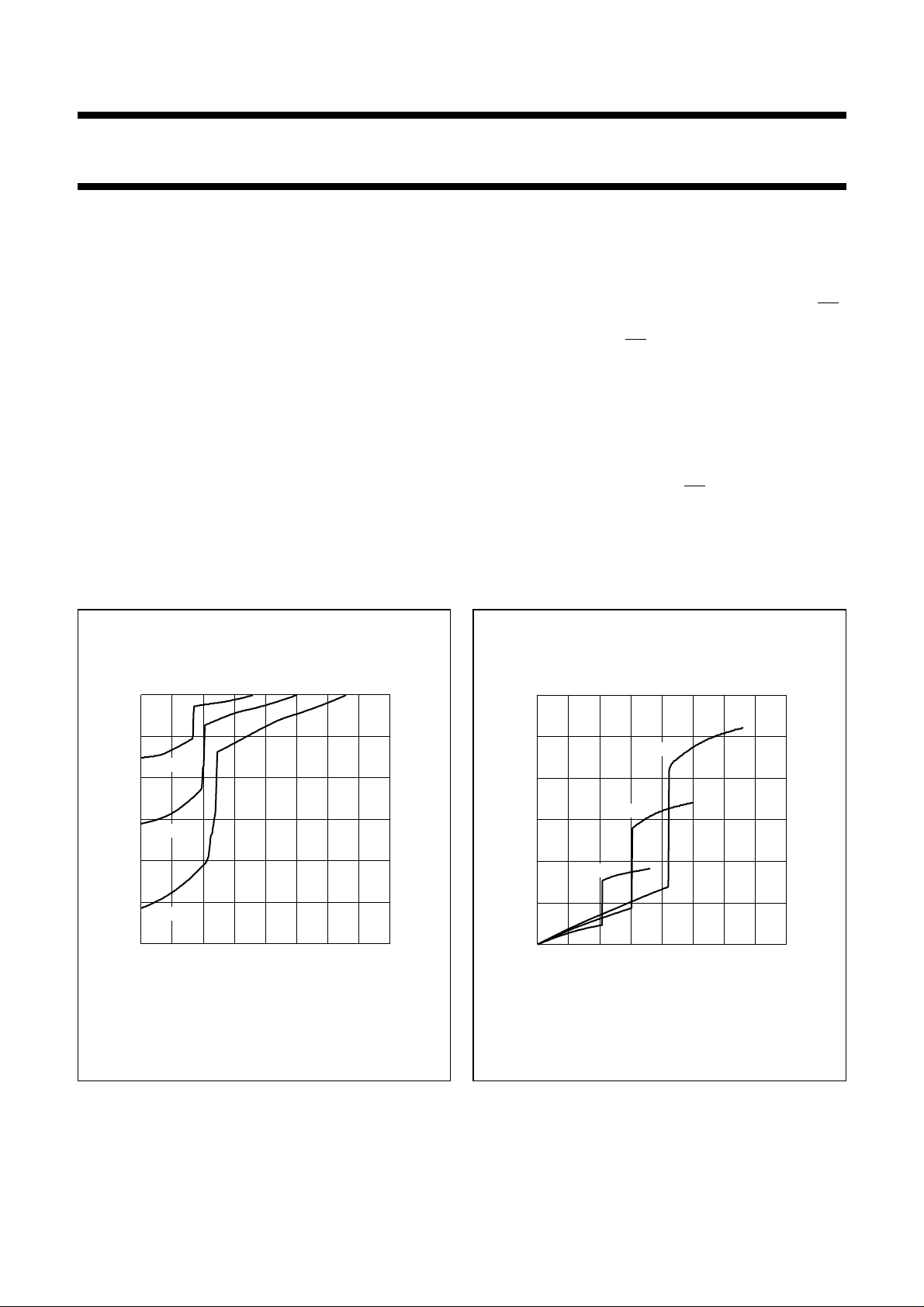
VOH (V)
MNA506
handbook, halfpage
0
I
OH
(mA)
−100
−200
−300
012 4
1.8 V
2.5 V
3.3 V
Fig.1 Output current as function of output voltage.
3
MNA507
VOL (V)
300
handbook, halfpage
I
OL
(mA)
200
100
0
012 4
3.3 V
2.5 V
1.8 V
Fig.2 Output current as function of output voltage.
1999 Nov 15 2

Philips Semiconductors Product specification
16-bit transceiver with direction pin; 3-state
74AVC16245
(3.6 V tolerant)
QUICK REFERENCE DATA
GND = 0 V; T
SYMBOL PARAMETER CONDITIONS TYP. UNIT
t
PHL/tPLH
C
I
C
PD
Notes
1. C
is used to determine the dynamic power dissipation (PDin µW).
PD
PD=CPD× V
fi= input frequency in MHz;
fo= output frequency in MHz;
CL= output load capacitance in pF;
VCC= supply voltage in Volts;
∑ (CL× V
2. The condition is VI= GND to VCC.
=25°C; tr=tf≤2.0 ns; CL=30pF.
amb
propagation delay nAnto nBn;
nBnto nA
n
VCC= 1.2 V 2.8 ns
V
= 1.5 V 1.8 ns
CC
V
= 1.8 V 1.8 ns
CC
= 2.5 V 1.3 ns
V
CC
V
= 3.3 V 1.1 ns
CC
input capacitance 5.0 pF
power dissipation capacitance per buffer notes 1 and 2
outputs enabled 42 pF
outputs disabled 2 pF
2
× fi+ ∑ (CL× V
CC
2
× fo) = sum of outputs.
CC
2
× fo) where:
CC
FUNCTION TABLE
See note 1.
INPUTS INPUTS/OUTPUTS
n
OE nDIR nA
L L A = B inputs
L H inputs B = A
HXZZ
Note
1. H = HIGH voltage level;
L = LOW voltage level;
X = don’t care;
Z = high-impedance OFF-state.
n
nB
n
1999 Nov 15 3

Philips Semiconductors Product specification
16-bit transceiver with direction pin; 3-state
74AVC16245
(3.6 V tolerant)
ORDERING INFORMATION
TYPE NUMBER
TEMPERATURE RANGE PINS PACKAGE MATERIAL CODE
74AVC16245DGG −40 to +85 °C 48 TSSOP plastic SOT362-1
PINNING
PIN SYMBOL DESCRIPTION
1 1DIR direction control
2, 3, 5, 6, 8, 9, 11 and 12 1B
to 1B
0
4, 10, 15, 21, 28, 34, 39 and 45 GND ground (0 V)
7, 18, 31 and 42 V
13, 14, 16, 17, 19, 20, 22 and 23 2B
CC
to 2B
0
24 2DIR direction control
25 2
26, 27, 29, 30, 32, 33, 35 and 36 2A
37, 38, 40, 41, 43, 44, 46 and 47 1A
48 1
OE output enable input (active LOW)
to 2A
7
to 1A
7
OE output enable input (active LOW)
PACKAGE
7
7
0
0
data inputs/outputs
DC supply voltage
data inputs/outputs
data inputs/outputs
data inputs/outputs
1999 Nov 15 4

Philips Semiconductors Product specification
16-bit transceiver with direction pin; 3-state
(3.6 V tolerant)
handbook, halfpage
1DIR
1B
1B
GND
1B
1B
V
CC
1B
1B
GND
1B
1B
2B
2B
GND
2B
2B
V
CC
2B
2B
GND
2B
2B
2DIR
1
2
0
3
1
4
5
2
6
3
7
8
4
9
5
10
11
6
12
7
0
1
2
3
4
5
6
7
16245
13
14
15
16
17
18
19
20
21
22
23
24
MNA508
1OE
48
1A
47
0
1A
46
1
GND
45
1A
44
2
1A
43
3
V
42
CC
1A
41
4
1A
40
5
GND
39
1A
38
6
1A
37
7
2A
36
0
2A
35
1
GND
34
2A
33
2
2A
32
3
V
31
CC
2A
30
4
2A
29
5
GND
28
2A
27
6
26
2A
7
25
2OE
1OE
1DIR
2OE
2DIR
1A
1A
1A
1A
1A
1A
1A6
1A
2A
2A
2A
2A
2A
2A
2A
2A
74AVC16245
48
G3
1
3EN1[BA]
3EN2[AB]
25
G6
24
6EN1[BA]
6EN2[AB]
47
0
46
1
44
2
43
3
41
4
40
5
38
37
7
36
0
35
1
33
2
32
3
30
4
29
5
27
6
26
7
1
2
4
5
2
1B
3
1B
5
1B
6
1B
8
1B
9
1B
11
1B
12
1B
13
2B
14
2B
16
2B
17
2B
19
2B
20
2B
22
2B
23
2B
MNA003
0
1
2
3
4
5
6
7
0
1
2
3
4
5
6
7
Fig.3 Pin configuration.
1999 Nov 15 5
Fig.4 IEEE/IEC logic symbol.
 Loading...