

Philips 74AUC1G08 Technical data
INTEGRATED CIRCUITS
DATA SH EET
74AUC1G08
Single 2-input AND gate
Preliminary specification
File under Integrated Circuits, IC24
2002 Nov 12
Philips Semiconductors Preliminary specification
Single 2-input AND gate 74AUC1G08
FEATURES
• Wide supply voltage range from 0.8 to 2.7 V
• Performance optimised for VCC= 1.8 V
• High noise immunity
• Complies with JEDEC standard:
– JESD76 (1.65 to 1.95 V)
• ESD protection:
– HBM EIA/JESD22-A114-A exceeds 2000 V
– MM EIA/JESD22-A115-A exceeds 200 V
• 8 mA output drive (VCC= 1.65 V)
DESCRIPTION
The 74AUC1G08 is a high-performance, low-power,
low-voltage, Si-gate CMOS device.
Schmitt-trigger action at all inputs makes the circuit
tolerant for slower input rise and fall time.
This device is fully specified for partial power-down
applications usingI
. The I
off
circuitry disablesthe output,
off
preventing the damaging current backflow through the
device when it is powered down.
The 74AUC1G08 provides the single 2-input AND
function.
• CMOS low power consumption
• Latch-up performance exceeds 250 mA
• 3.3 V tolerant inputs/outputs
• SC-88A and SC-74A package.
QUICK REFERENCE DATA
GND = 0 V; T
=25°C; input slewrate ≥ 1 V/ns.
amb
SYMBOL PARAMETER CONDITIONS TYPICAL UNIT
t
PHL/tPLH
propagation delay inputs A and B to
output Y
VCC= 0.8 V; CL= 15 pF; RL=2kΩ 4.7 ns
VCC= 1.2 V; CL= 15 pF; RL=2kΩ 1.9 ns
VCC= 1.5 V; CL= 15 pF; RL=2kΩ 1.4 ns
V
= 1.8 V; CL= 30 pF; RL=1 kΩ 1.4 ns
CC
VCC= 2.5 V; CL= 30 pF; RL= 500 Ω 1.2 ns
C
I
C
PD
input capacitance 4 pF
power dissipation capacitance per buffer VCC= 1.8 V; notes 1 and 2 14 pF
Notes
1. C
is used to determine the dynamic power dissipation (PDin µW).
PD
PD=CPD× V
2
× fi+(CL× V
CC
2
× fo) where:
CC
fi= input frequency in MHz;
fo= output frequency in MHz;
CL= output load capacitance in pF;
VCC= supply voltage in Volts.
2. The condition is VI= GND to VCC.
2002 Nov 12 2
Philips Semiconductors Preliminary specification
Single 2-input AND gate 74AUC1G08
FUNCTION TABLE
See note 1.
INPUT OUTPUT
ABY
LLL
LHL
HLL
HHH
Note
1. H = HIGH voltage level;
L = LOW voltage level.
ORDERING INFORMATION
PACKAGE
TYPE NUMBER
74AUC1G08GW −40 to +85 °C 5 SC-88A plastic SOT353 FE
74AUC1G08GV −40 to +85 °C 5 SC-74A plastic SOT753 F08
TEMPERATURE
RANGE
PINS PACKAGE MATERIAL CODE MARKING
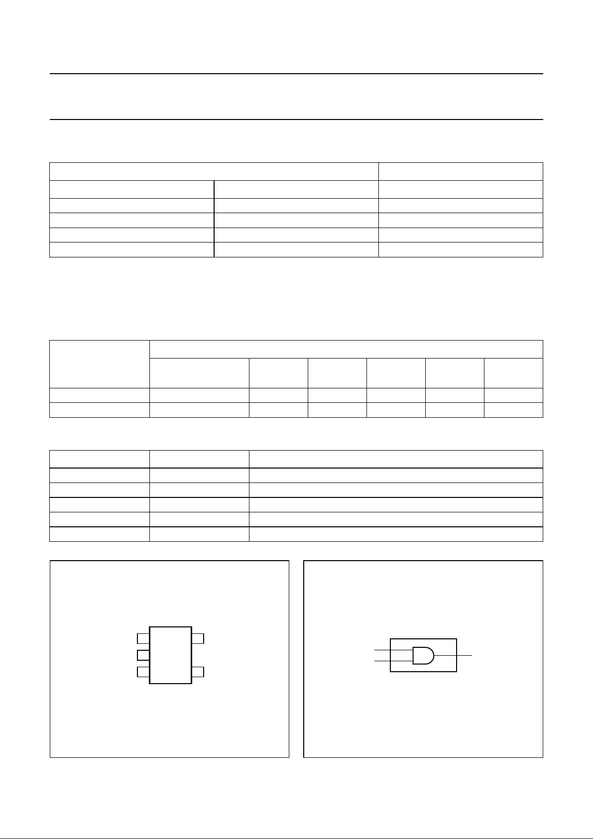
PINNING
handbook, halfpage
PIN SYMBOL DESCRIPTION
1 B data input B
2 A data input A
3 GND ground (0 V)
4 Y data output Y
5V
B
A
GND
CC
1
2
3
5
08
4
MNA112
V
CC
Y
supply voltage
handbook, halfpage
1
B
2
A
Y
MNA113
4
Fig.1 Pin configuration.
2002 Nov 12 3
Fig.2 Logic symbol.
Philips Semiconductors Preliminary specification
Single 2-input AND gate 74AUC1G08
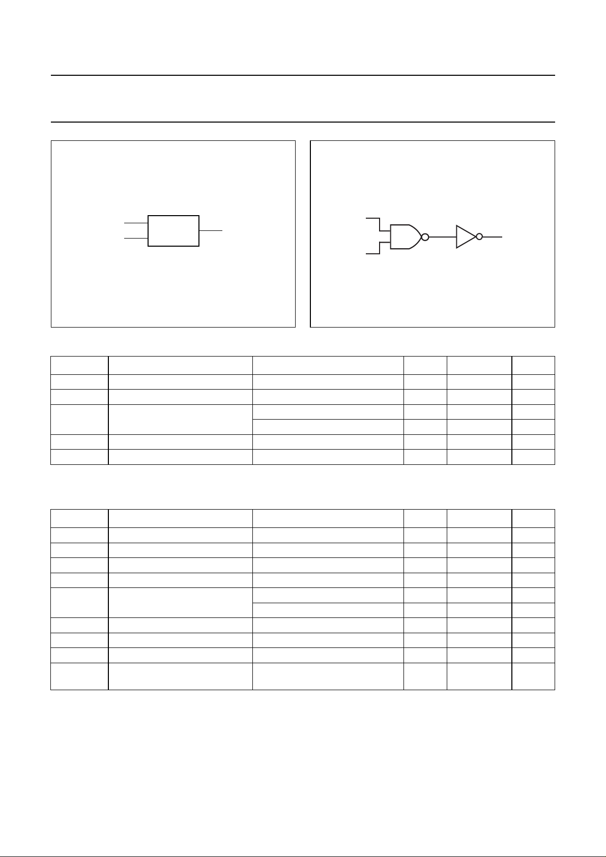
handbook, halfpage
1
2
&
4
MNA114
Fig.3 IEE/IEC logic symbol.
A
Y
B
Fig.4 Logic diagram.
RECOMMENDED OPERATING CONDITIONS
SYMBOL PARAMETER CONDITIONS MIN. MAX. UNIT
V
CC
V
I
V
O
supply voltage 0.8 2.7 V
input voltage 0 2.7 V
output voltage active mode 0 V
CC
V
VCC= 0 V; Power-down mode 0 2.7 V
T
amb
operating ambient temperature −40 +85 °C
tr,tf (∆t/∆f) input rise and fall times 0 20 ns/V
LIMITING VALUES
In accordance with theAbsolute Maximum Rating System (IEC 60134); voltages are referenced to GND (ground = 0 V).
SYMBOL PARAMETER CONDITIONS MIN. MAX. UNIT
V
CC
I
IK
V
I
I
OK
V
O
supply voltage −0.5 +3.6 V
input diode current VI<0 −−50 mA
input voltage note 1 −0.5 +3.6 V
output diode current VO>VCC or VO<0 −±50 mA
output voltage active mode; notes 1 and 2 −0.5 VCC+ 0.5 V
Power-down mode; notes 1 and 2 −0.5 +3.6 V
I
O
ICC, I
T
stg
P
D
GND
output source or sink current VO=0toV
CC
−±60 mA
VCC or GND current −±100 mA
storage temperature −65 +150 °C
power dissipation per package for temperature range from
− 250 mW
−40 to +85 °C
Notes
1. The input and output voltage ratings may be exceeded if the input and output current ratings are observed.
2. When VCC=0 (Powered-down mode), the output voltage can be 2.7 V in normal operation.
2002 Nov 12 4
 Loading...