

Philips 74ALVT16953DL, 74ALVT16953DGG Datasheet

INTEGRATED CIRCUITS
74ALVT16953
2.5V/3.3V 16-bit registered transceiver
(3-State)
Product specification
Supersedes data of 1995 Sep 19
IC23 Data Handbook
1998 Mar 26
Philips Semiconductors Product specification
SYMBOL
PARAMETER
UNIT
74AL VT169532.5V/3.3V 16-bit registered transceiver (3-State)
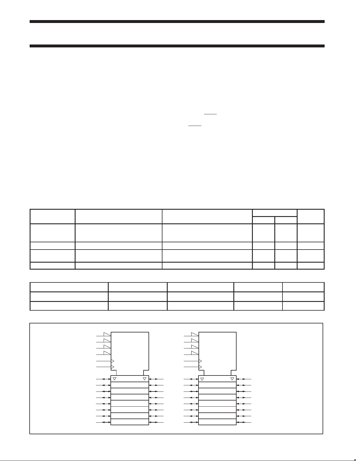
FEA TURES
•Two 8-bit registered transceivers
•5V I/O Compatible
•3-State buffers
•Output capability: +64mA/–32mA
•TTL input and output switching levels
•Input and output interface capability to systems at 5V supply
•Bus hold data inputs eliminate the need for external pull-up
resistors to hold unused inputs
•Live insertion/extraction permitted
•Power-up 3-State
•Power-up reset
•No bus current loading when output is tied to 5V bus
•Latch-up protection exceeds 500mA per JEDEC Std 17
•ESD protection exceeds 2000V per MIL STD 883 Method 3015
and 200V per Machine Model
QUICK REFERENCE DATA
t
PLH
t
PHL
C
C
I
CCZ
IN
I/O
Propagation delay
nCPBA to nAx or
nCPAB to nBx
Input capacitance VI = 0V or V
I/O pin capacitance
Total supply current Outputs disabled 40 70 µA
DESCRIPTION
The 74ALVT16953 is a high-performance BiCMOS product
designed for V
to 5V .
The 74ALVT16953 is a dual octal registered inverting transceiver.
Two 8-bit registers store data flowing in both directions between two
bidirectional buses. Data applied to the inputs is entered and stored
on the rising edge of the Clock (nCPXX) provided that the Clock
Enable (nCEXX
output buffers, but is only accessible when the Output Enable
(nOEXX
for B inputs to A outputs.
Active bus hold circuitry is provided to hold unused or floating data
inputs at a valid logic level.
CONDITIONS
T
= 25°C; GND = 0V
amb
CL = 50pF;
CC
V
= 0V or V
I/O
Outputs disabled
operation at 2.5V or 3.3V with I/O compatibility up
CC
) is Low. The data is then present at the 3-State
) is Low. Data flow from A inputs to B outputs is the same as
TYPICAL
2.5V 3.3V
3.0
3.0
2.2
2.3
3 3 pF
CC
9 9 pF
ns
ORDERING INFORMATION
PACKAGES TEMPERATURE RANGE OUTSIDE NORTH AMERICA NORTH AMERICA DWG NUMBER
56-Pin Plastic SSOP Type III –40°C to +85°C 74ALVT16953 DL AV16953 DL SOT371-1
56-Pin Plastic TSSOP Type II –40°C to +85°C 74ALVT16953 DGG AV16953 DGG SOT364-1
LOGIC SYMBOL (IEEE/IEC)
3
54
56
55
5
6
8
9
10
12
13
14
EN1
EN2
EN3
1
EN4
2
C5
C6
2, 3, 6
1, 4, 5
52
51
49
48
47
45
44
43
1998 Mar 26 853-2054 19170
26
31
29
28
27
30
15
16
17
19
20
21
23
24
EN1
EN2
EN3
EN4
C5
C6
1, 4, 52, 3, 6
42
41
40
38
37
36
34
33
SH00069
2
Philips Semiconductors Product specification
74ALVT169532.5V/3.3V 16-bit registered transceiver (3-State)
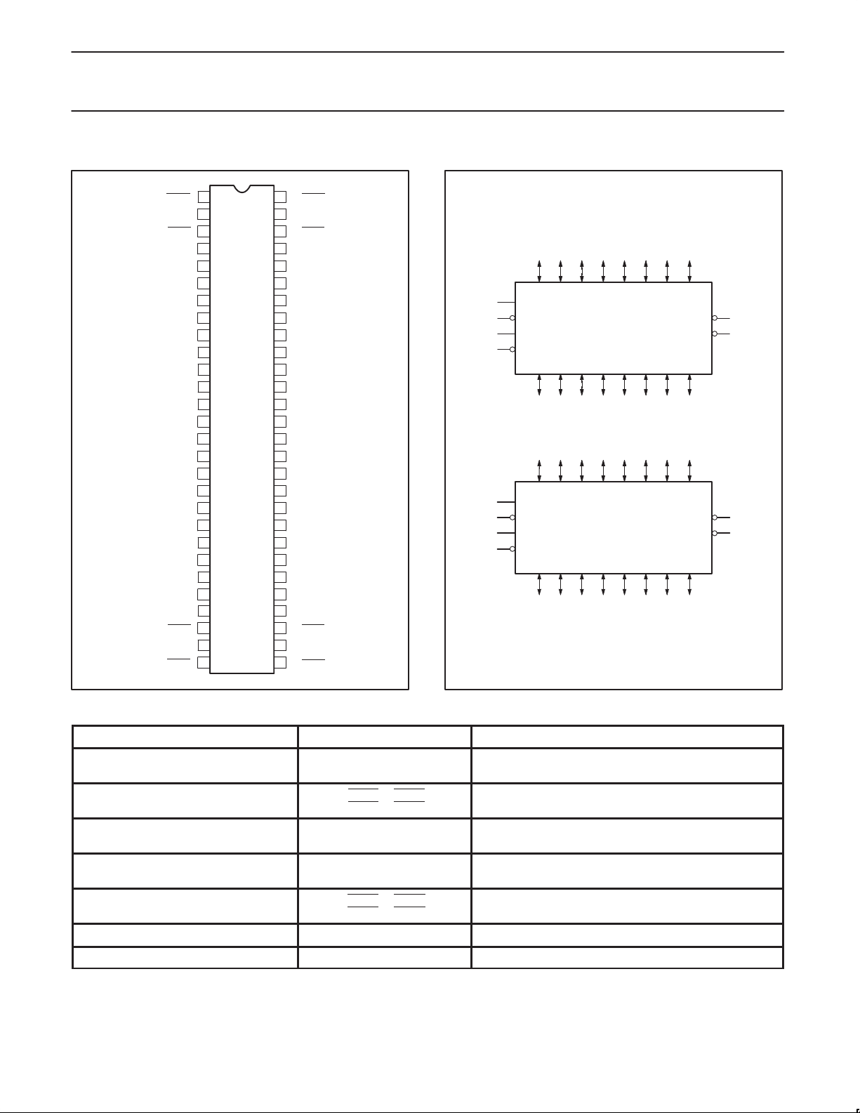
PIN CONFIGURATION
1
1OEAB
2
1CPAB
1CEAB
3
GND
4
1A0
5
1A1
6
7
V
CC
8
1A2
1A3
9
1A4
10
GND
11
1A5
12
1A6
13
1A7
14
2A0
15
16
2A1
2A2
17
GND
18
2A3
19
20
2A4
21
2A5
22
V
CC
23
2A6
24
2A7
25
GND
26
2CEAB
27
2CPAB
28
2OEAB
SH00070
LOGIC SYMBOL
56
1OEBA
55
1CPBA
1CEBA
54
GND
53
1B0
52
1B1
51
50
V
CC
49
1B2
1B3
48
1B4
47
GND
46
1B5
45
1B6
44
1B7
43
2B0
42
41
2B1
2B2
40
GND
39
2B3
38
37
2B4
36
2B5
35
V
CC
34
2B6
33
2B7
32
GND
31
2CEBA
30
2CPBA
29
2OEBA
2
3
55
54
27
26
30
31
568910121314
1A0 1A1 1A2 1A3 1A4 1A5 1A6 1A7
1CPAB
1CEAB
1CPBA
1CEBA
1B0 1B1 1B2 1B3 1B4 1B5 1B6 1B7
52 51 49 48 47 45 44 43
15 16 17 19 20 21 23 24
2A0 2A1 2A2 2A3 2A4 2A5 2A6 2A7
2CPAB
2CEAB
2CPBA
2CEBA
2B0 2B1 2B2 2B3 2B4 2B5 2B6 2B7
42 41 40 38 37 36 34 33
561OEBA
11OEAB
292OEBA
282OEAB
SH00071
PIN DESCRIPTION
PIN NUMBER SYMBOL NAME AND FUNCTION
2, 55
27, 30
3, 54,
26, 31
5, 6, 8, 9, 10, 12, 13, 14, 15,
16, 17, 19, 20, 21, 23, 24
52, 51, 49, 48, 47, 45, 44, 43
42, 41, 40, 38, 37, 36, 34, 33
1, 56
28, 29
4, 11, 18, 25, 32, 39, 46, 53 GND Ground (0V)
7, 22, 35, 50 V
1998 Mar 26
1CPAB / 1CPBA
2CPAB / 2CPBA
1CEAB / 1CEBA
2CEAB / 2CEBA
1A0 – 1A7
2A0 – 2A7
1B0 – 1B7
2B0 – 2B7
1OEAB / 1OEBA
2OEAB / 2OEBA
CC
Clock input A to B / Clock input B to A
Clock enable input A to B / Clock enable input B to A
Data inputs/outputs (A side)
Data inputs/outputs (B side)
Output enable inputs
Positive supply voltage
3

Philips Semiconductors Product specification
INTERNAL
OPERATING
74ALVT169532.5V/3.3V 16-bit registered transceiver (3-State)
FUNCTION TABLE for Register nAx or nBx
INPUTS
nAx or
nBx
nCPXX nCEXX
Q
X X H NC Hold data
L
H
↑
↑
L
L
H
L
Load data
H =High voltage level
L =Low voltage level
↑ =Low-to-High transition
X = Don’t care
XX= AB or BA
NC=No change
LOGIC DIAGRAM
nCEAB
nCPAB
nOEAB
CE
nA0
D
CP
MODE
Q
FUNCTION TABLE for Output Enable
INPUTS
nOEXX
H X Z Disable outputs
L
L
H =High voltage level
L =Low voltage level
X = Don’t care
XX= AB or BA
Z =High impedance ”off” state
INTERNAL nAx or nBx OPERATING
Q OUTPUTS MODE
L
H
H
L
DETAIL A
Enable outputs
nA1
nA2
nA3
nA4
nA5
nA6
nA7
nOEBA
nCEBA
nCPBA
DETAIL A X 7
CE
Q
CP
D
nB0
nB1
nB2
nB3
nB4
nB5
nB6
nB7
SH00126
1998 Mar 26
4

Philips Semiconductors Product specification
SYMBOL
PARAMETER
UNIT
I
mA
74ALVT169532.5V/3.3V 16-bit registered transceiver (3-State)
ABSOLUTE MAXIMUM RATINGS
SYMBOL
V
CC
I
IK
V
I
I
OK
V
OUT
I
OUT
T
stg
DC supply voltage –0.5 to +4.6 V
DC input diode current VI < 0 –50 mA
DC input voltage
DC output diode current VO < 0 –50 mA
DC output voltage
DC output current output in Low state
Storage temperature range –65 to +150 °C
PARAMETER CONDITIONS RATING UNIT
3
3
1, 2
–0.5 to +7.0 V
output in Off or High state –0.5 to +7.0 V
output in High state
128
–64
mA
NOTES:
1. Stresses beyond those listed may cause permanent damage to the device. These are stress ratings only and functional operation of the
device at these or any other conditions beyond those indicated under “recommended operating conditions” is not implied. Exposure to
absolute-maximum-rated conditions for extended periods may affect device reliability .
2. The performance capability of a high-performance integrated circuit in conjunction with its thermal environment can create junction
temperatures which are detrimental to reliability. The maximum junction temperature of this integrated circuit should not exceed 150°C.
3. The input and output voltage ratings may be exceeded if the input and output current ratings are observed.
RECOMMENDED OPERATING CONDITIONS
2.5V RANGE LIMITS 3.3V RANGE LIMITS
MIN MAX MIN MAX
V
CC
V
V
V
I
OH
OL
∆t/∆v Input transition rise or fall rate; Outputs enabled 10 10 ns/V
T
amb
DC supply voltage 2.3 2.7 3.0 3.6 V
Input voltage 0 5.5 0 5.5 V
I
High-level input voltage 1.7 2.0 V
IH
Input voltage 0.7 0.8 V
IL
High-level output current –8 –32 mA
Low-level output current 8 32
Low-level output current; current duty cycle ≤ 50%; f ≥ 1kHz 24 64
Operating free-air temperature range –40 +85 –40 +85 °C
1998 Mar 26
5
 Loading...