

Philips 74ALVT16899DL, 74ALVT16899DGG Datasheet

74ALVT16899
2.5V/3.3V 18-bit latched transceiver with
16-bit parity generator/checker (3-State)
Product specification
IC23 Data Handbook
1998 Jun 30
INTEGRATED CIRCUITS
Philips Semiconductors Product specification
74AL VT16899
2.5V/3.3V 18-bit latched transceiver with
16-bit parity generator/checker (3-State)
2
1998 Jun 30 853-2090-19651
FEATURES
•Symmetrical (A and B bus functions are identical)
•Selectable generate parity or ”feed-through” parity for A-to-B and
B-to-A directions
•Independent transparent latches for A-to-B and B-to-A directions
•Selectable ODD/EVEN parity
•Continuously checks parity of both A bus and B bus latches as
ERRA
and ERRB
•Open-collector ERR output
•Ability to simultaneously generate and check parity
•Can simultaneously read/latch A and B bus data
•Output capability: +64 mA/–32mA
•Latch-up protection exceeds 500mA per Jedec Std 17
•ESD protection exceeds 2000 V per MIL STD 883 Method 3015
and 200 V per Machine Model
•Power up 3-State
•Power-up reset
•No bus current loading when output is tied to 5 V bus
•Live insertion/extraction permitted
•Bus-hold data inputs eliminate the need for external pull-up
resistors to hold unused inputs
DESCRIPTION
The 74ALVT16899 is a high-performance BiCMOS product
designed for V
CC
operation at 2.5V or 3.3V with I/O compatibility up
to 5V .
The 74ALVT16899 is a 16-bit to 16-bit parity transceiver with
separate transparent latches for the A bus and B bus. Either bus
can generate or check parity. The parity bit can be fed-through with
no change or the generated parity can be substituted with the SEL
input.
The 74ALVT16899 features independent latch enables for the A and
B bus latches, a select pin for ODD/EVEN parity, and separate error
signal output pins for checking parity.
FUNCTIONAL DESCRIPTION:
The 74ALVT16899 has three principal modes of operation which are
outlined below. All modes apply to both the A-to-B and B-to-A
directions.
Transparent latch, Generate parity, Check A and B bus parity:
Bus A (B) communicates to Bus B (A), parity is generated and
passed on to the B (A) Bus as BPAR (APAR). If LEA and LEB are
High and the Mode Select (SEL
) is Low, the parity generated from
A0-A7 and B0-B7 can be checked and monitored by ERRA
and
ERRB
. (Fault detection on both input and output buses.)
Transparent latch, Feed-through parity, Check A and B bus
parity:
Bus A (B) communicates to Bus B (A) in a feed-through mode if SEL
is High. Parity is still generated and checked as ERRA and ERRB
and can be used as an interrupt to signal a data/parity bit error to the
CPU.
Latched input, Generate/Feed-through parity, Check A (and B)
bus parity:
Independent latch enables (LEA and LEB) allow other permutations
of:
•Transparent latch / 1 bus latched / both buses latched
•Feed-through parity / generate parity
•Check in bus parity / check out bus parity / check in and out bus
parity
QUICK REFERENCE DA TA
CONDITIONS
TYPICAL
SYMBOL
PARAMETER
CONDITIONS
T
amb
= 25°C; GND = 0V
2.5 V
3.3 V
UNIT
t
PLH
t
PHL
Propagation delay
An to Bn or Bn to An
CL = 50pF
2.0
2.2
1.5
1.7
ns
t
PLH
t
PHL
Propagation delay
An to ERRA
CL = 50pF
9.8
7.0
7.8
5.1
ns
C
IN
Input capacitance VI = 0V or V
CC
3 3 pF
C
I/O
Output capacitance Outputs disabled; VO = 0V or V
CC
9 9 pF
I
CCZ
Quiescent supply current Outputs disabled 40 70 µA
ORDERING INFORMATION
PACKAGES TEMPERATURE RANGE OUTSIDE NORTH AMERICA NORTH AMERICA DWG NUMBER
56-Pin Plastic SSOP Type III –40°C to +85°C 74ALVT16899 AV16899 DL SOT371-1
56-Pin Plastic TSSOP Type II –40°C to +85°C 74ALVT16899 DGG AV16899 DGG SOT364-1
Philips Semiconductors Product specification
74AL VT16899
2.5V/3.3V 18-bit latched transceiver with 16-bit parity
generator/checker (3-State)
1998 Jun 30
3
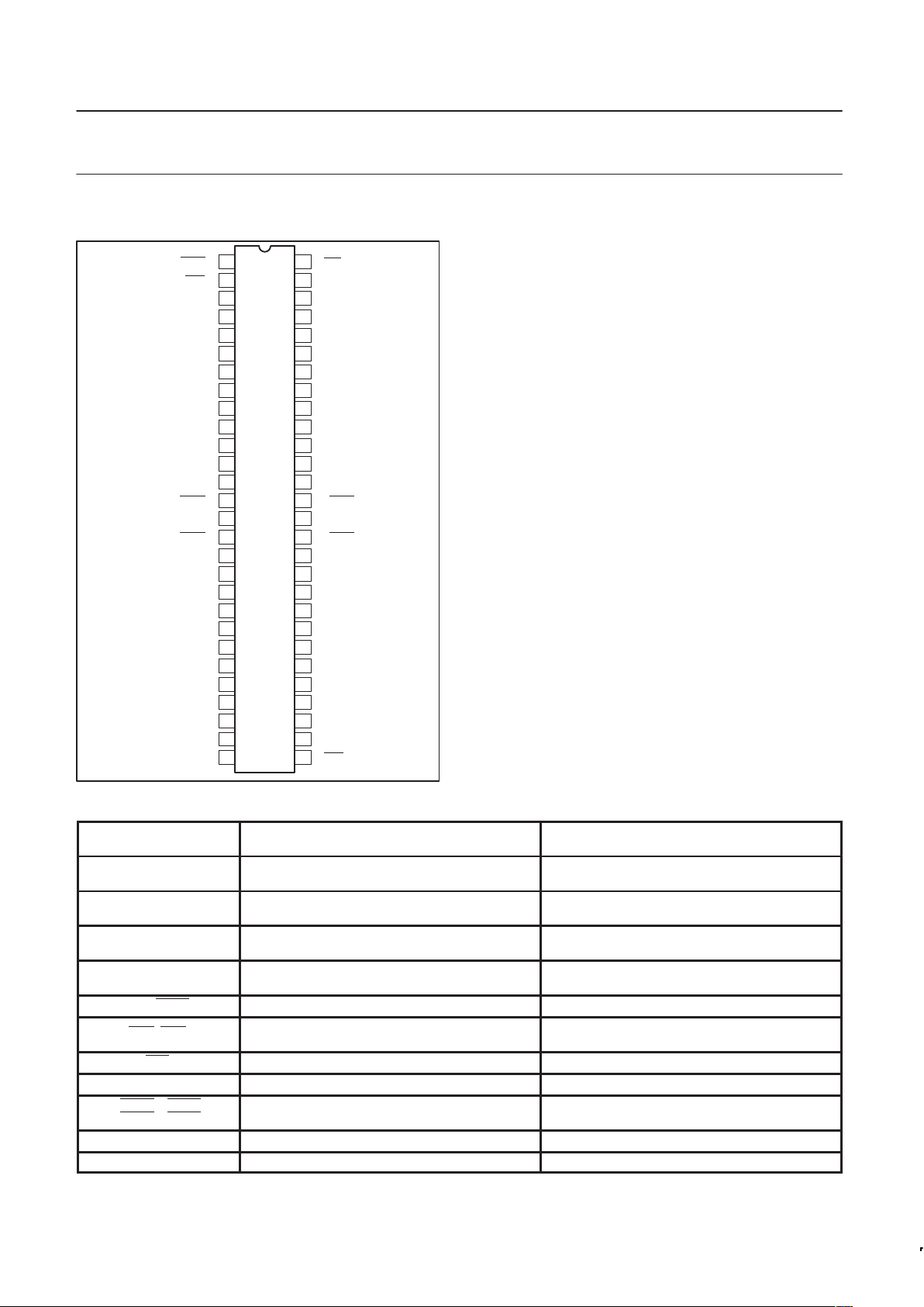
PIN CONFIGURATION
SV01731
GND
1B6
SEL
GND
OEA
ODD/EVEN
1A6
1A3 1B3
2A7 2B7
2A4 2B4
2B1
OEB
2A1
LEB
2A0
1
2
3
4
5
6
7
8
9
10
11
12
13
14
15
16
17
18
19
20
21
22
23
24
25
26
27
28 29
30
31
32
33
34
35
36
37
38
39
40
41
42
43
44
45
46
47
48
49
50
51
52
53
54
55
56
1A0
1A1
1A2
1A4
V
CC
1A5
1A7
1APAR
1ERRA
GND
2ERRA
2APAR
2A6
2A5
V
CC
2A3
2A2
GND
LEA
1B0
1B2
1B1
1B4
V
CC
1B5
1B7
1BPAR
1ERRB
GND
2ERRB
2BPAR
2B6
2B5
V
CC
2B3
2B2
GND
2B0
PIN DESCRIPTION
SYMBOL
PIN
NUMBER
NAME AND FUNCTION
1A0 - 1A7
2A0 - 2A7
3, 5, 6, 7, 8, 10, 11, 12
27, 25, 24, 23, 22, 20, 19, 18
Latched A bus 3-State inputs/outputs
1B0 - 1B7
2B0 - 2B7
54, 52, 51, 50, 49, 47, 46, 45
30, 32, 33, 34, 35, 37, 38, 39
Latched B bus 3-State inputs/outputs
1APAR
2APAR
13, 17 A bus parity 3-State input/output
1BPAR
2BPAR
44, 40 B bus parity 3-State input/output
ODD/EVEN 1 Parity select input (Low for EVEN parity)
OEA, OEB 2, 29
Output enable inputs (gate A to B,
B to A)
SEL 56 Mode select input (Low for generate)
LEA, LEB 55, 28 Latch enable inputs (transparent High)
1ERRA, 1ERRB
2ERRA, 2ERRB
14, 43,
16, 41
Error signal outputs (active-Low)
GND 4, 15, 26, 31, 42, 53 Ground (0V)
V
CC
9, 21, 36, 48 Positive supply voltage
Philips Semiconductors Product specification
74AL VT16899
2.5V/3.3V 18-bit latched transceiver with 16-bit parity
generator/checker (3-State)
1998 Jun 30
4
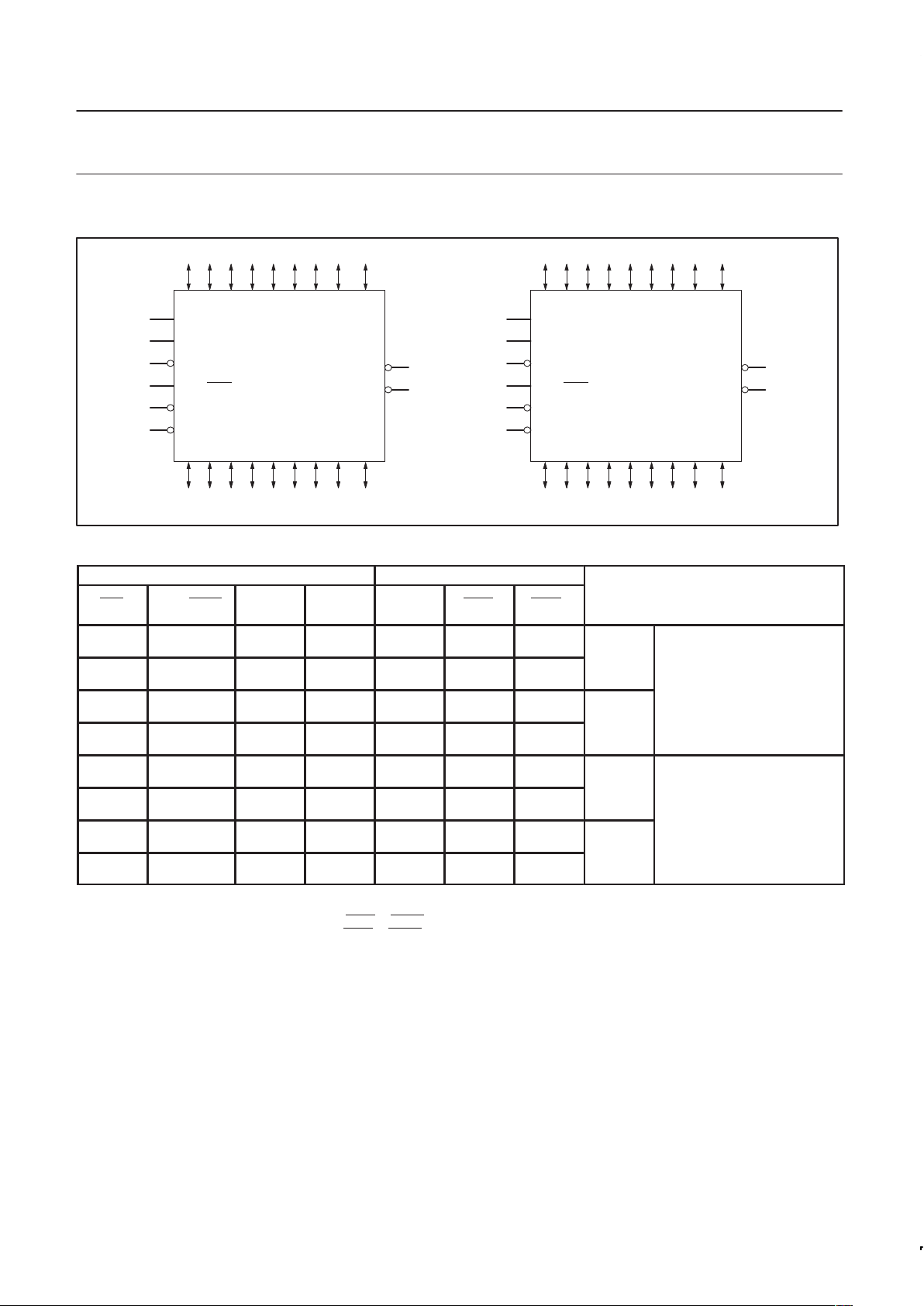
LOGIC SYMBOL
3 5 6 7 8 10 11 12
1A0 1A1 1A2 1A3 1A4 1A5 1A6 1A7
1B0 1B1 1B2 1B3 1B4 1B5 1B6 1B7
54 52 51 50 49 47 46 45
14
43
55
56
28
1
LEA
SEL
LEB
ODD/EVEN
1ERRA
1ERRB
13
1APAR
1BPAR
44
2
29 OEB
OEA
SH00083
27 25 24 23 22 20 19 18
2A0 2A1 2A2 2A3 2A4 2A5 2A6 2A7
2B0 2B1 2B2 2B3 2B4 2B5 2B6 2B7
30 32 33 34 35 37 38 39
16
41
55
56
28
1
LEA
SEL
LEB
ODD/EVEN
2ERRA
2ERRB
17
2APAR
2BPAR
40
2
29
OEB
OEA
PARITY AND ERROR FUNCTION TABLE
INPUTS OUTPUTS
SEL ODD/EVEN
xPAR
(A or B)
Σ of High
Inputs
xPAR
(B or A)
ERRt ERRr*
PARITY MODES
H H H
Even
Odd
H
H
H
L
H
L Odd
H H L
Even
Odd
L
L
L
H
L
H
Mode
Feed-through/check parity
H L H
Even
Odd
H
H
L
H
L
H Even
H L L
Even
Odd
L
L
H
L
H
L
Mode
L H H
Even
Odd
H
L
H
L
H
H Odd
L H L
Even
Odd
H
L
L
H
H
H
Mode
Generate parity
L L H
Even
Odd
L
H
L
H
H
H Even
L L L
Even
Odd
L
H
H
L
H
H
Mode
H = High voltage level
L = Low voltage level
t = Transmit–if the data path is from A→B then ERRt
is ERRA
r = Receive–if the data path is from A→B then ERRr is ERRB
* Blocked if latch is not transparent
Philips Semiconductors Product specification
74AL VT16899
2.5V/3.3V 18-bit latched transceiver with 16-bit parity
generator/checker (3-State)
1998 Jun 30
5
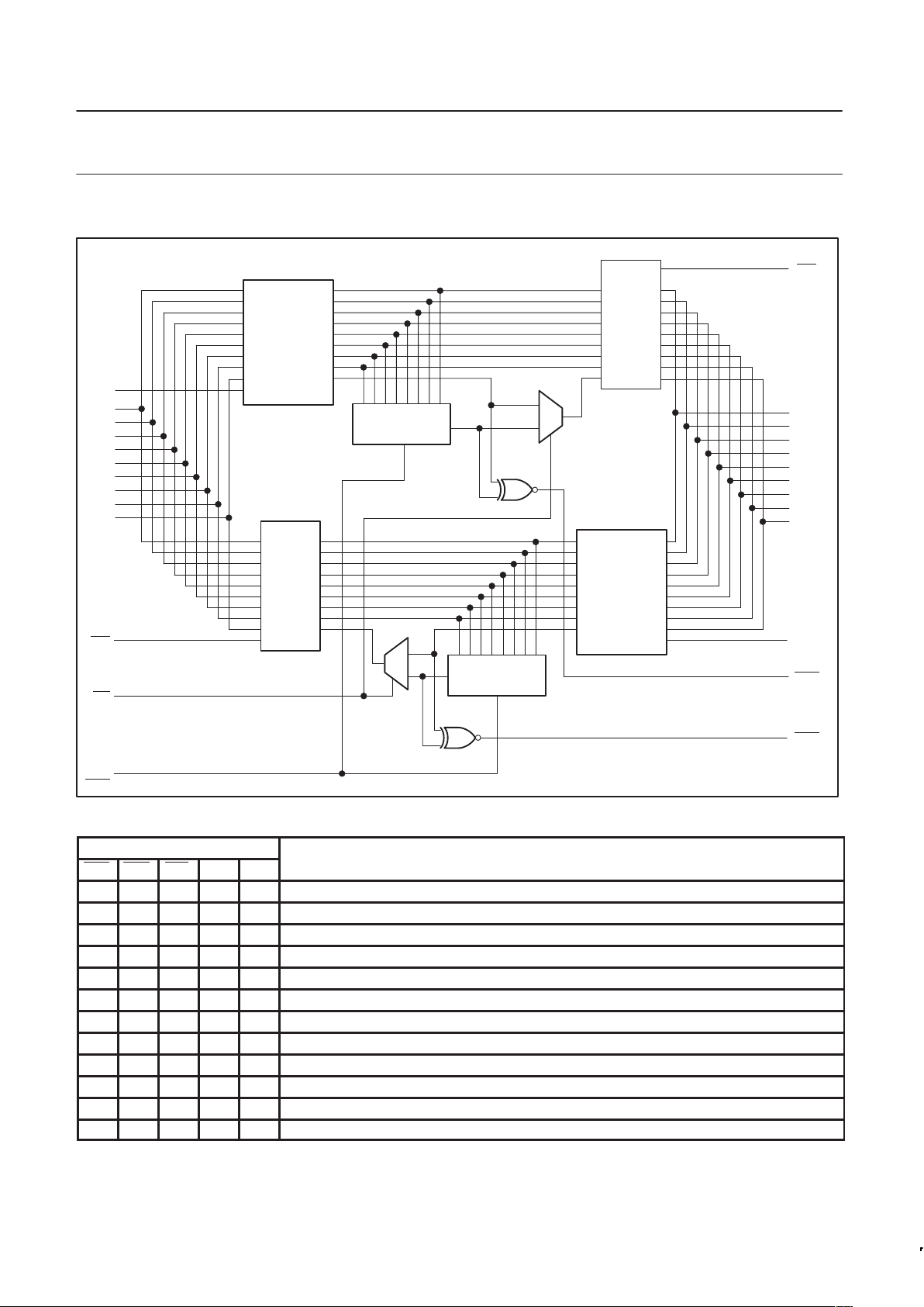
BLOCK DIAGRAM
1
0
mux
9–bit
Output
Buffer
OE
9–bit
Output
Buffer
9–bit
Transparent
Latch
LE
Parity
Generator
Parity
Generator
1
0
mux
OE
9–bit
Transparent
Latch
LE
OEB
LEA
A0
A1
A2
A3
A4
A5
A6
A7
APAR
OEA
SEL
ODD/
EVEN
LEB
B7
BPAR
B6
B5
B4
B3
B2
B1
B0
ERRA
ERRB
SH00084
(1 of 2 parity blocks)
FUNCTION TABLE
INPUTS OPERATING MODE
OEB OEA SEL LEA LEB
H H X X X 3-State A bus and B bus (input A & B simultaneously)
H L L L H B → A, transparent B latch, generate parity from B0 - B7, check B bus parity
H L L H H B → A, transparent A & B latch, generate parity from B0 - B7, check A & B bus parity
H L L X L B → A, B bus latched, generate parity from latched B0 - B7 data, check B bus parity
H L H X H B → A, transparent B latch, parity feed-through, check B bus parity
H L H H H B → A, transparent A & B latch, parity feed-through, check A & B bus parity
L H L H X A → B, transparent A latch, generate parity from A0 - A7, check A bus parity
L H L H H A → B, transparent A & B latch, generate parity from A0 - A7, check A & B bus parity
L H L L X A → B, A bus latched, generate parity from latched A0 - A7 data, check A bus parity
L H H H L A → B, transparent A latch, parity feed-through, check A bus parity
L H H H H A → B, transparent A & B latch, parity feed-through, check A & B bus parity
L L X X X Output to A bus and B bus (NOT ALLOWED)
H = High voltage level
L = Low voltage level
X = Don’t care

Philips Semiconductors Product specification
74AL VT16899
2.5V/3.3V 18-bit latched transceiver with 16-bit parity
generator/checker (3-State)
1998 Jun 30
6
ABSOLUTE MAXIMUM RATINGS
1, 2
SYMBOL
PARAMETER CONDITIONS RATING UNIT
V
CC
DC supply voltage -0.5 to +4.6 V
I
IK
DC input diode current VI < 0 -50 mA
V
I
DC input voltage
3
-0.5 to +7.0 V
I
OK
DC output diode current VO < 0 -50 mA
V
OUT
DC output voltage
3
Output in Off or High state -0.5 to +7.0 V
p
Output in Low state 128
I
OUT
DC out ut current
Output in High state -64
mA
T
stg
Storage temperature range -65 to +150 °C
NOTES:
1. Stresses beyond those listed may cause permanent damage to the device. These are stress ratings only and functional operation of the
device at these or any other conditions beyond those indicated under “recommended operating conditions” is not implied. Exposure to
absolute-maximum-rated conditions for extended periods may affect device reliability .
2. The performance capability of a high-performance integrated circuit in conjunction with its thermal environment can create junction
temperatures which are detrimental to reliability. The maximum junction temperature of this integrated circuit should not exceed 150°C.
3. The input and output negative voltage ratings may be exceeded if the input and output clamp current ratings are observed.
RECOMMENDED OPERATING CONDITIONS
2.5V RANGE LIMITS 3.3V RANGE LIMITS
SYMBOL
PARAMETER
MIN MAX MIN MAX
UNIT
V
CC
DC supply voltage 2.3 2.7 3.0 3.6 V
V
I
Input voltage 0 5.5 0 5.5 V
V
IH
High-level input voltage 1.7 2.0 V
V
IL
Input voltage 0.7 0.8 V
I
OH
High-level output current –8 –32 mA
Low-level output current 8 32
I
OL
Low-level output current; current duty cycle ≤ 50%; f ≥ 1kHz 24 64
mA
∆t/∆v Input transition rise or fall rate; Outputs enabled 10 10 ns/V
T
amb
Operating free-air temperature range –40 +85 –40 +85 °C
 Loading...