

Philips 74ALVT16821DL, 74ALVT16821DGG Datasheet
INTEGRATED CIRCUITS
74ALVT16821
20-bit bus-interface D-type flip-flop;
positive-edge trigger (3-State)
Product specification
Supersedes data of 1997 May 01
IC24 Data Handbook
1998 Feb 13
Philips Semiconductors Product specification
SYMBOL
PARAMETER
UNIT
2.5V/3.3V 20-bit bus-interface D-type flip-flop;
positive-edge trigger (3-State)
FEA TURES
•20-bit positive-edge triggered register
•5V I/O Compatible
•Multiple V
and GND pins minimize switching noise
CC
•Live insertion/extraction permitted
•Power-up reset
•Power-up 3-State
•Output capability: +64mA/-32mA
•Latch-up protection exceeds 500mA per Jedec Std 17
•ESD protection exceeds 2000V per MIL STD 883 Method 3015
and 200V per Machine Model
•Bus hold data inputs eliminate the need for external pull-up
resistors to hold unused inputs
QUICK REFERENCE DATA
C
t
PLH
t
PHL
C
OUT
I
CCZ
IN
Propagation delay
nCP to nQ
Input capacitance VI = 0V or V
Output capacitance VO = 0 or V
Total supply current Outputs disabled 40 70 µA
CL = 50pF
DESCRIPTION
The 74ALVT16821 high-performance BiCMOS device combines
low static and dynamic power dissipation with high speed and high
output drive. It is designed for V
compatibility to 5V .
The 74ALVT16821 has two 10-bit, edge triggered registers, with
each register coupled to a 3-State output buffer. The two sections of
each register are controlled independently by the clock (nCP) and
Output Enable (nOE
Each register is fully edge triggered. The state of each D input, one
set-up time before the Low-to-High clock transition, is transferred to
the corresponding flip-flop’s Q output.
The 3-State output buffers are designed to drive heavily loaded
3-State buses, MOS memories, or MOS microprocessors.
The active Low Output Enable (nOE
independent of the register operation. When nOE
the register appears at the outputs. When nOE
are in high impedance “off” state, which means they will neither drive
nor load the bus.
CONDITIONS
T
CC
CC
amb
= 25°C
CC
) control gates.
74AL VT16821
operation at 2.5V or 3.3V with I/O
) controls all ten 3-State buffers
is Low, the data in
is High, the outputs
TYPICAL
2.5V 3.3V
2.6
2.7
3 3 pF
9 9 pF
1.7
1.8
ns
ORDERING INFORMATION
PACKAGES TEMPERATURE RANGE OUTSIDE NORTH AMERICA NORTH AMERICA DWG NUMBER
56-Pin Plastic SSOP Type III –40°C to +85°C 74ALVT16821 DL AV16821 DL SOT371-1
56-Pin Plastic TSSOP Type II –40°C to +85°C 74ALVT16821 DGG AV16821 DGG SOT364-1
1998 Feb 13 853-1869 18962
2
Philips Semiconductors Product specification
2.5V/3.3V 20-bit bus-interface D-type flip-flop;
positive-edge trigger (3-State)
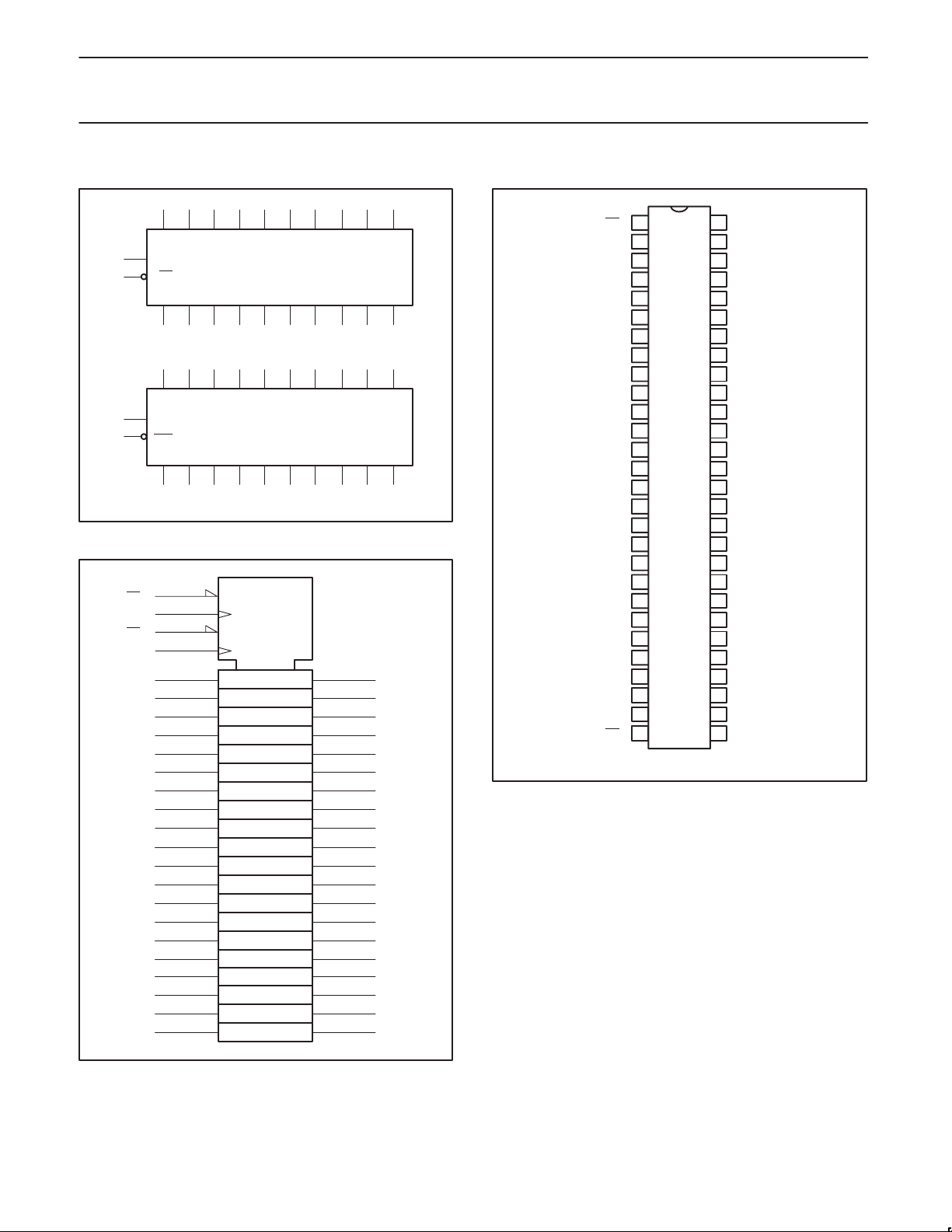
LOGIC SYMBOL
56 54 52 51 49 48 47 45 44 43
1D0 1D1 1D2 1D3 1D4 1D5 1D6 1D7
1CP
56
1OE
1
1Q0 1Q1 1Q2 1Q3 1Q4 1Q5 1Q6 1Q7
2 3 5 6 8 9 10 12 13 14
42 41 40 38 37 36 34 33 31 30
2D0 2D1 2D2 2D3 2D4 2D5 2D6 2D7
29
2CP
28
2OE
2Q0 2Q1 2Q2 2Q3 2Q4 2Q5 2Q6 2Q7
15 16 17 19 20 21 23 24 26 27
LOGIC SYMBOL (IEEE/IEC)
1OE
1CP
2OE
2CP
1D0
1D1
1D2
1D3
1D4
1D5
1D6
1D7
1D8
1D9
2D0
2D1
2D2
2D3
2D4
2D5
2D6
2D7
2D8
2D9
1
56
28
29
55
54
52
51
49
48
47
45
44
43
42
41
40
38
37
36
34
33
31
30
EN2
C1
EN4
C3
1D
3D
2 ∇
4 ∇
1D8 1D9
1Q8 1Q9
2D8 2D9
2Q8 2Q9
SH00002
2
3
5
6
8
9
10
12
13
14
15
16
17
19
20
21
23
24
26
27
SH00003
1Q0
1Q1
1Q2
1Q3
1Q4
1Q5
1Q6
1Q7
1Q8
1Q9
2Q0
2Q1
2Q2
2Q3
2Q4
2Q5
2Q6
2Q7
2Q8
2Q9
PIN CONFIGURATION
1
2
1Q0
3
1Q1
4
GND
5
1Q2
6
1Q3
7
V
CC
8
1Q4
9
1Q5
10
1Q6
11
GND
12
1Q7
13
1Q8
14
1Q9
15
2Q0
16
2Q1
17
2Q2
18
GND
19
2Q3
20
2Q4
21
2Q5
22
V
CC
23
2Q6
24
2Q7
25
GND
26
2Q8
27
2Q9
28 29
2OE
74ALVT16821
561OE
1CP
55
1D0
54
1D1
53
GND
52
1D2
51
1D3
50
V
CC
49
1D4
48
1D5
47
1D6
46
GND
45
1D7
44
1D8
43
1D9
42
2D0
41
2D1
40
2D2
39
GND
38
2D3
37
2D4
36
2D5
35
V
CC
34
2D6
33
2D7
32
GND
31
2D8
30
2D9
2CP
SH00001
1998 Feb 13
3
Philips Semiconductors Product specification
INTERNAL
OPERATING
2.5V/3.3V 20-bit bus-interface D-type flip-flop;
positive-edge trigger (3-State)
PIN DESCRIPTION
PIN NUMBER SYMBOL FUNCTION
56, 54, 52, 51, 49,
48, 47, 45, 44, 43,
42, 41, 40, 38, 37,
36, 34, 33, 31, 30
2, 3, 5, 6, 8, 9, 10,
12, 13, 14,
15, 16, 17, 19, 20,
21, 23, 24, 26, 27
1, 28 1OE, 2OE
56, 29 1CP, 2CP
4, 11, 18, 25, 32,
39, 46, 53
7, 22, 35, 50 V
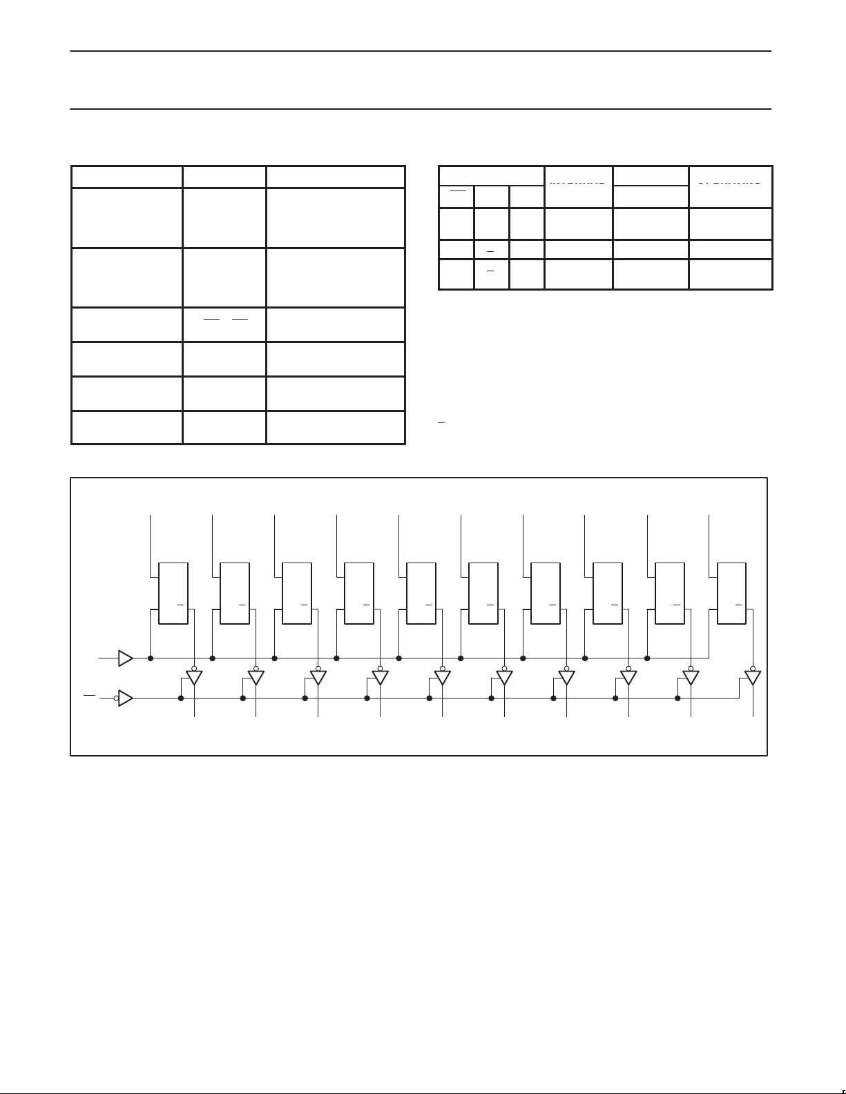
LOGIC DIAGRAM
1D0 - 1D9
2D0 - 2D9
1Q0 - 1Q9
2Q0 - 2Q9
Data inputs
Data outputs
Output enable inputs
(active-Low)
Clock pulse inputs
(active rising edge)
GND Ground (0V)
CC
Positive supply
voltage
74ALVT16821
FUNCTION TABLE
INPUTS
nOE nCP nDx
L
↑
L
↑
l
h
INTERNAL
REGISTER
L
H
L ↑ X NC NC Hold
H
↑
H
↑XDn
NC
Dn
H = High voltage level
h = High voltage level one set-up time prior to the Low-to-High
clock transition
L = Low voltage level
l = Low voltage level one set-up time prior to the Low-to-High
clock transition
NC= No change
X = Don’t care
Z = High impedance “off” state
↑ = Low to High clock transition
= Not a Low-to-High clock transition
↑
OUTPUTS
nQ0 - nQ9
L
H
Z
Z
OPERATING
MODE
Load and read
register
Disable
outputs
nCP
nOE
nD0
D
CP Q
nQ0
nD1
D
CP Q
nQ1
nD2
D
CP Q
nQ2
nD3
D
CPQ
nQ3
nD4
D
CP Q
nQ4
nD5
D
CPQ
nQ5
nD6
D
CP Q
nQ6
nD7
D
CPQ
nQ7
nD8
D
CPQ
nQ8
nD9
D
CPQ
nQ9
SH00004
1998 Feb 13
4
 Loading...