

Philips 74ALVT16652DL, 74ALVT16652DGG Datasheet

INTEGRATED CIRCUITS
74ALVT16652
2.5V/3.3V 16-bit bus transceiver/register
(3-State)
Product specification
Supersedes data of 1996 Aug 13
IC23 Data Handbook
1998 Feb 13
Philips Semiconductors Product specification
SYMBOL
PARAMETER
UNIT
2.5V/3.3V 16-bit bus transceiver/register
(3-State)
FEA TURES
•16–bit bus interface
•5V I/O Compatible
•3-State buffers
•Output capability: +64mA/-32mA
•TTL input and output switching levels
•Input and output interface capability to systems at 5V supply
•Bus-hold data inputs eliminate the need for external pull-up
resistors to hold unused inputs
•Live insertion/extraction permitted
•Power-up reset
•Power-up 3-State
•No bus current loading when output is tied to 5V bus
•Latch-up protection exceeds 500mA per JEDEC JC40.2 Std 17
•ESD protection exceeds 2000V per MIL STD 883 Method 3015
and 200V per Machine Model
QUICK REFERENCE DATA
t
PLH
t
PHL
C
C
I
CCZ
IN
I/O
Propagation delay
nAx to nBx or nBx to nAx
CL = 50pF
Input capacitance DIR, OE VI = 0V or V
I/O pin capacitance V
= 0V or V
I/O
Total supply current Outputs disabled 40 70 µA
74AL VT16652
DESCRIPTION
The 74ALVT16652 is a high-performance BiCMOS product
designed for V
to 5V. The device can be used as two 8-bit transceivers or one
16-bit transceiver.
Complimentary output-enable (OEAB and OEBA
provided to control the transceiver functions. Select-control (SAB
and SBA) inputs are provided to select whether real-time or stored
data is transferred. A Low-input level selects real-time data, and a
High input level selects stored data. The circuitry used for select
control eliminates the typical decoding glitch that occurs in a
multiplexer during the transition between stored and real-time data.
Data on the A or B bus, or both, can be stored in the internal
flip-flops by Low-to-High transitions at the appropriate clock (CPAB
or CPBA) inputs regardless of the levels on the select-control or
output-enable inputs. When SAB and SBA are in real-time transfer
mode, it is possible to store data without using the internal D-type
flip-flops by simultaneously enabling OEAB and OEBA
configuration, each output reinforces its input. Thus, when all other
data sources to the two sets of bus lines are at high impedance,
each set of bus lines remains at its last level configuration.
CONDITIONS
T
amb
CC
CC
operation at 2.5V or 3.3V with I/O compatibility up
CC
) inputs are
TYPICAL
= 25°C
2.5V 3.3V
2.0
2.1
1.5
1.6
3 3 pF
9 9 pF
. In this
ns
ORDERING INFORMATION
PACKAGES TEMPERATURE RANGE OUTSIDE NORTH AMERICA NORTH AMERICA DWG NUMBER
56-Pin Plastic SSOP Type III –40°C to +85°C 74ALVT16652 DL AV16652 DL SOT371-1
56-Pin Plastic TSSOP Type II –40°C to +85°C 74ALVT16652 DGG AV16652 DGG SOT364-1
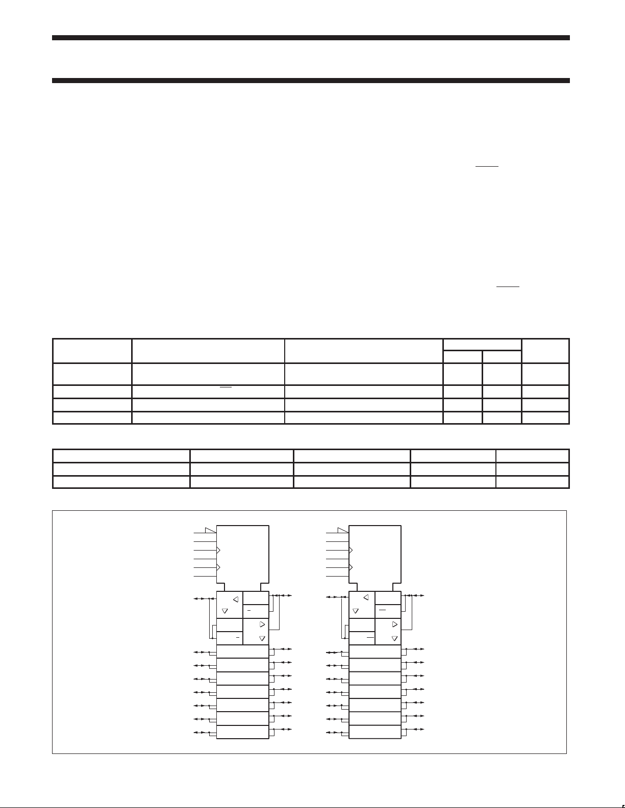
LOGIC SYMBOL (IEEE/IEC)
56
1
55
54
2
3
5
6
8
9
10
12
13
14
EN1(BA)
EN2(AB)
C3
G4
C5
G6
1
1
5D 6
16
43D
4
1
1
2
29
28
30
31
27
26
52
15
51
16
49
17
48
19
47
20
45
21
44
23
43
24
EN7(BA)
EN8(AB)
C9
G10
C11
G12
1
7
11D 12
1
12
10 9D
10
1
8
42
1
41
40
38
37
36
34
33
SW00158
1998 Feb 13 853-1854 18962
2

Philips Semiconductors Product specification
2.5V/3.3V 16-bit bus transceiver/register
(3-State)
PIN CONFIGURATION
1OEAB
1CPAB
1SAB
GND
1A0
1A1
V
CC
1A2
1A3
1A4
GND
1A5
1A6
1A7
2A0
2A1
2A2
GND
2A3
2A4
2A5
V
CC
2A6
2A7
GND
2SAB
2CPAB
20EAB
1
2
3
4
5
6
7
8
9
10
11
12
13
14
15
16
17
18
19
20
21
22
23
24
25
26
27
28
SH00046
1OE
56
BA
1CPBA
55
54
1SBA
53
GND
52
1B0
51
1B1
50
V
CC
49
1B2
48
1B3
47
1B4
46
GND
45
1B5
44
1B6
43
1B7
42
2B0
41
2B1
40
2B2
39
GND
38
2B3
37
2B4
36
2B5
35
V
CC
34
2B6
33
2B7
32
GND
31
2SBA
30
2CPBA
29
2OE
BA
LOGIC SYMBOL
2
3
54 1SBA
55 1CPBA
27
26
31
30
74ALVT16652
5 6 8 9 10 12 13 14
1A0 1A1 1A2 1A3 1A4 1A5 1A6 1A7
1CPAB
1SAB
1AB 1B1 1B2 1B3 1B4 1B5 1B6 1B7
52 51 49 48 47 45 44 43
15 16 17 19 20 21 23 24
2A0 2A1 2A2 2A3 2A4 2A5 2A6 2A7
2CPAB
2SAB
2SBA
2CPBA
2AB 2B1 2B2 2B3 2B4 2B5 2B6 2B7
42 41 40 38 37 36 34 33
2OEAB
2OEBA
11OEAB
561OEBA
28
29
SW00159
PIN DESCRIPTION
PIN NUMBER SYMBOL NAME AND FUNCTION
2, 55, 27, 30 1CPAB, 1CPBA, 2CPAB, 2CPBA Clock input A to B / Clock input B to A
3, 54, 26, 31 1SAB, 1SBA, 2SAB, 2SBA Select input A to B / Select input B to A
5, 6, 8, 9, 10, 12, 13, 14
15, 16, 17, 19, 20, 21, 23, 24
52, 51, 49, 48, 47, 45, 44, 43
42, 41, 40, 38, 37, 36, 34, 33
1, 56, 28, 29
4, 11, 18, 25, 32, 39, 46, 53 GND Ground (0V)
7, 22, 35, 50 V
1998 Feb 13
1A0 – 1A7,
2A0 – 2A7
1B0 – 1B7,
2B0 – 2B7
1OEAB, 1OEBA,
2OEAB, 2OEBA
CC
3
Data inputs/outputs (A side)
Data inputs/outputs (B side)
Output enable inputs
Positive supply voltage

Philips Semiconductors Product specification
OPERATING MODE
2.5V/3.3V 16-bit bus transceiver/register
(3-State)
LOGIC DIAGRAM
nOE
BA
nOEAB
nCPBA
nSBA
nCPAB
nSAB
1of 8 Channels
nA0
1D
C1
Q
74ALVT16652
1D
C1
Q
nB0
nA1 nB1
nA2
nA3
nA4
nA5
nA6
nA7
DETAIL A X 7
nB2
nB3
nB4
nB5
nB6
nB7
SH00065
FUNCTION TABLE
INPUTS DATA I/O
nOEAB nOEBA nCPAB nCPBA nSAB nSBA nAx nBx
L
L
X
H
L
L
L
L
H
H
H L H or L H or L H H Output Output
H = High voltage level
L = Low voltage level
X = Don’t care
↑ = Low-to-High clock transition
* The data output function may be enabled or disabled by various signals at the nOEBA
always enabled, i.e., data at the bus pins will be stored on every Low-to-High transition of the clock.
** If both Select controls (nSAB and nSBA) are Low, then clocks can occur simultaneously. If either Select control is High, the clocks must
be staggered in order to load both registers.
H
H
H
H
X
L
L
L
H
H
H or L
↑
↑
↑
H or L
↑
X
X
X
H or L
H or L
↑
H or L
↑
↑
↑
X
H or L
X
X
X
X
X
**
X
X
X
X
L
H
X
X
X
X
X
**
L
H
X
X
Input Input
Input
Unspecified
Unspecified
output*
Output Input
Input Output
output*
Input
Isolation
Store A and B data
Store A, Hold B
Store A in both registers
Hold A, Store B
Store B in both registers
Real time B data to A bus
Stored B data to A bus
Real time A data to B bus
Store A data to B bus
Stored A data to B bus
Stored B data to A bus
and nOEAB inputs. Data input functions are
1998 Feb 13
4
Philips Semiconductors Product specification
2.5V/3.3V 16-bit bus transceiver/register
(3-State)
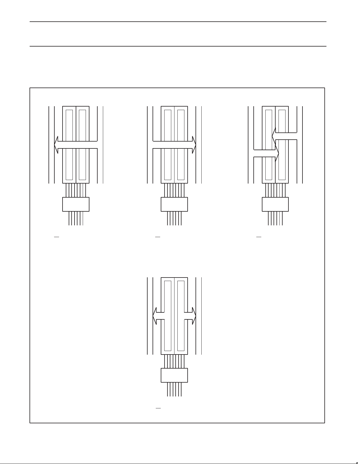
The following examples demonstrate the four fundamental
bus-management functions that can be performed with the
74ALVT16652. The select pins determine whether data is stored or
REAL TIME BUS TRANSFER
BUS B TO BUS A
ABAB AB
REAL TIME BUS TRANSFER
BUS A TO BUS B
74ALVT16652
transferred through the device in real time. The output enable pins
determine the direction of the data flow.
STORAGE FROM
A, B, OR A AND B
}
nOEAB nOEBA nCPAB nCPBA nSAB nSBA
LLXXXL
}
nOEAB nOEBA nCPAB nCPBA nSAB nSBA
HHXXLX
TRANSFER STORED DA TA
TO A OR B
AB
}
nOEAB nOEBA nCPAB nCPBA nSAB nSBA
XH↑ XXX
LXX↑ XX
LH↑↑XX
1998 Feb 13
}
nOEAB nOEBA nCPAB nCPBA nSAB nSBA
H L H | L H | L H H
SH00066
5
 Loading...