

Philips 74alvt16600 DATASHEETS

INTEGRATED CIRCUITS
74ALVT16600
2.5V/3.3V 18-bit universal bus
transceiver (3-State)
Product specification
Replaces data of 1997 May 12
IC23 Data Handbook
1998 Feb 13
Philips Semiconductors Product specification
SYMBOL
PARAMETER
UNIT
74AL VT166002.5V/3.3V 18-bit universal bus transceiver (3-State)
FEA TURES
•18-bit bidirectional bus interface
•5V I/O Compatible
•3-State buffers
•Output capability: +64mA/-32mA
•TTL input and output switching levels
•Input and output interface capability to systems at 5V supply
•Bus-hold data inputs eliminate the need for external pull-up
resistors to hold unused inputs
•Live insertion/extraction permitted
•Power-up reset
•Power-up 3-State
•No bus current loading when output is tied to 5V bus
•Negative edge-triggered clock inputs
•Latch-up protection exceeds 500mA per JEDEC JC40.2 Std 17
•ESD protection exceeds 2000V per MIL STD 883 Method 3015
and 200V per Machine Model
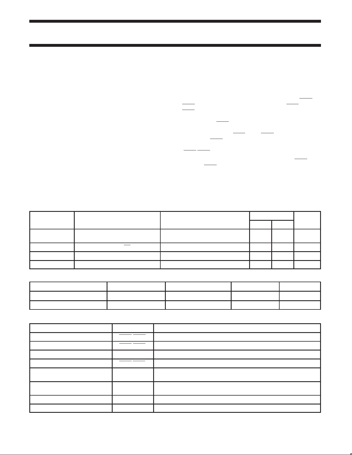
QUICK REFERENCE DATA
t
PLH
t
PHL
C
C
I
CCZ
IN
I/O
Propagation delay
An to Bn or Bn to An
Input capacitance DIR, OE VI = 0V or V
I/O pin capacitance Outputs disabled; V
Total supply current Outputs disabled 40 70 µA
CL = 50pF
DESCRIPTION
The 74ALVT16600 is a high-performance BiCMOS product
designed for V
up to 5V .
This device is an 18-bit universal transceiver featuring non-inverting
3-State bus compatible outputs in both send and receive directions.
Data flow in each direction is controlled by output enable (OEAB
OEBA
), latch enable (LEAB and LEBA), and clock (CPAB and
) inputs. For A-to-B data flow, the device operates in the
CPBA
transparent mode when LEAB is High. When LEAB is Low, the A
data is latched if CPAB
is Low, the A-bus data is stored in the latch/flip-flop on the
High-to-Low transition of CPAB
active. When OEAB
state. The High clock can be controlled with the clock-enable inputs
(CEBA
/CEAB).
Data flow for B-to-A is similar to that of A-to-B but uses OEBA
LEBA and CPBA
Active bus-hold circuitry is provided to hold unused or floating data
inputs at a valid logic level.
CONDITIONS
T
amb
CC
operation at 2.5V and 3.3V with I/O compatibility
CC
is held at a High or Low logic level. If LEAB
. When OEAB is Low, the outputs are
is High, the outputs are in the high-impedance
.
TYPICAL
= 25°C
= 0V or V
I/O
CC
2.5V 3.3V
1.9
2.5
4 4 pF
8 8 pF
1.6
1.9
and
,
ns
ORDERING INFORMATION
PACKAGES TEMPERATURE RANGE OUTSIDE NORTH AMERICA NORTH AMERICA DWG NUMBER
56-Pin Plastic SSOP Type III –40°C to +85°C 74ALVT16600 DL AV16600 DL SOT371-1
56-Pin Plastic TSSOP Type II –40°C to +85°C 74ALVT16600 DGG AV16600 DGG SOT364-1
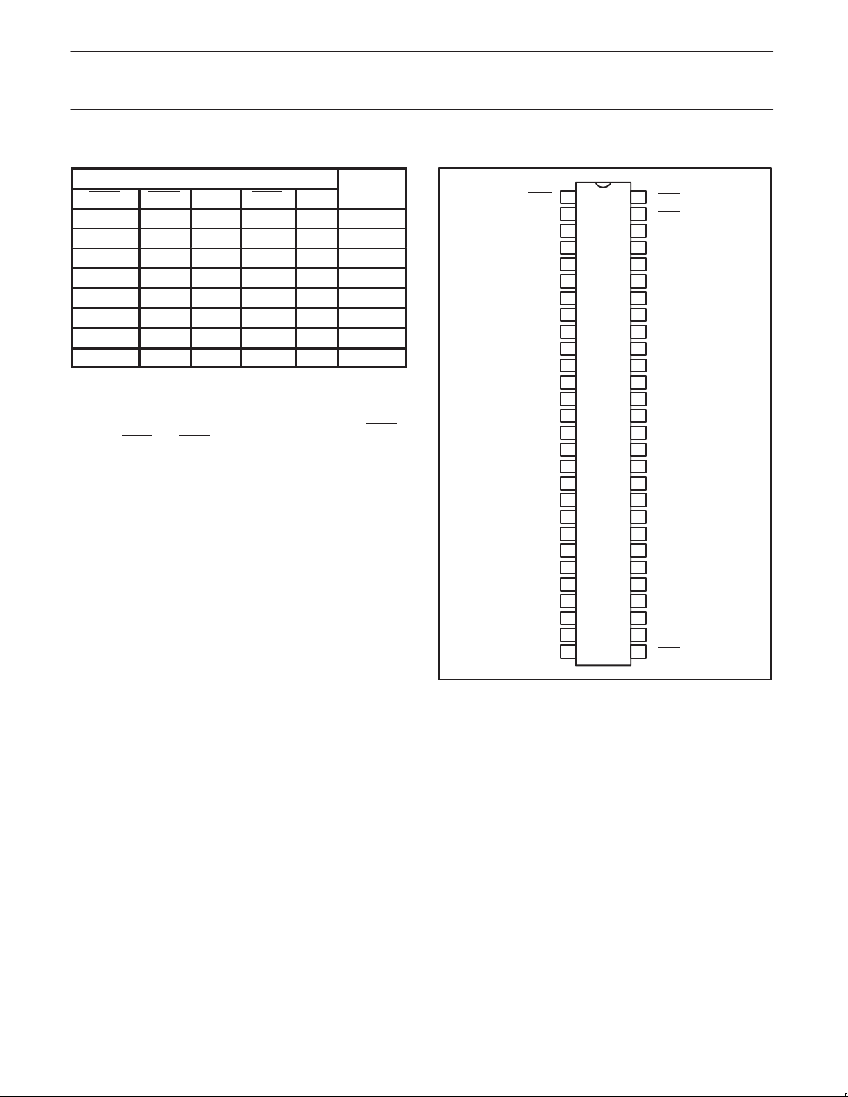
PIN DESCRIPTION
PIN NUMBER SYMBOL NAME AND FUNCTION
1, 27 OEAB/OEBA A-to-B Output enable input (active Low)
29, 56 CEBA/CEAB B-to-A / A-to-B clock enable (active Low)
2, 28 LEAB/LEBA A-to-B/B-to-A Latch enable input
55,30 CPAB/CPBA A-to-B/B-to-A Clock input (active falling edge)
3, 5, 6, 8, 9, 10, 12, 13, 14, 15,
16, 17, 19, 20, 21, 23, 24, 26
54, 52, 51, 49, 48, 47, 45, 44, 43,
42, 41, 40, 38, 37, 36, 34, 33, 31
4, 11, 18, 25, 32, 39, 46, 53 GND Ground (0V)
7, 22, 35, 50 V
1998 Feb 13 853-1979 18958
A0-A17 Data inputs/outputs (A side)
B0-B17 Data inputs/outputs (B side)
CC
Positive supply voltage
2
Philips Semiconductors Product specification
2.5V/3.3V 18-bit universal bus transceiver (3-State)
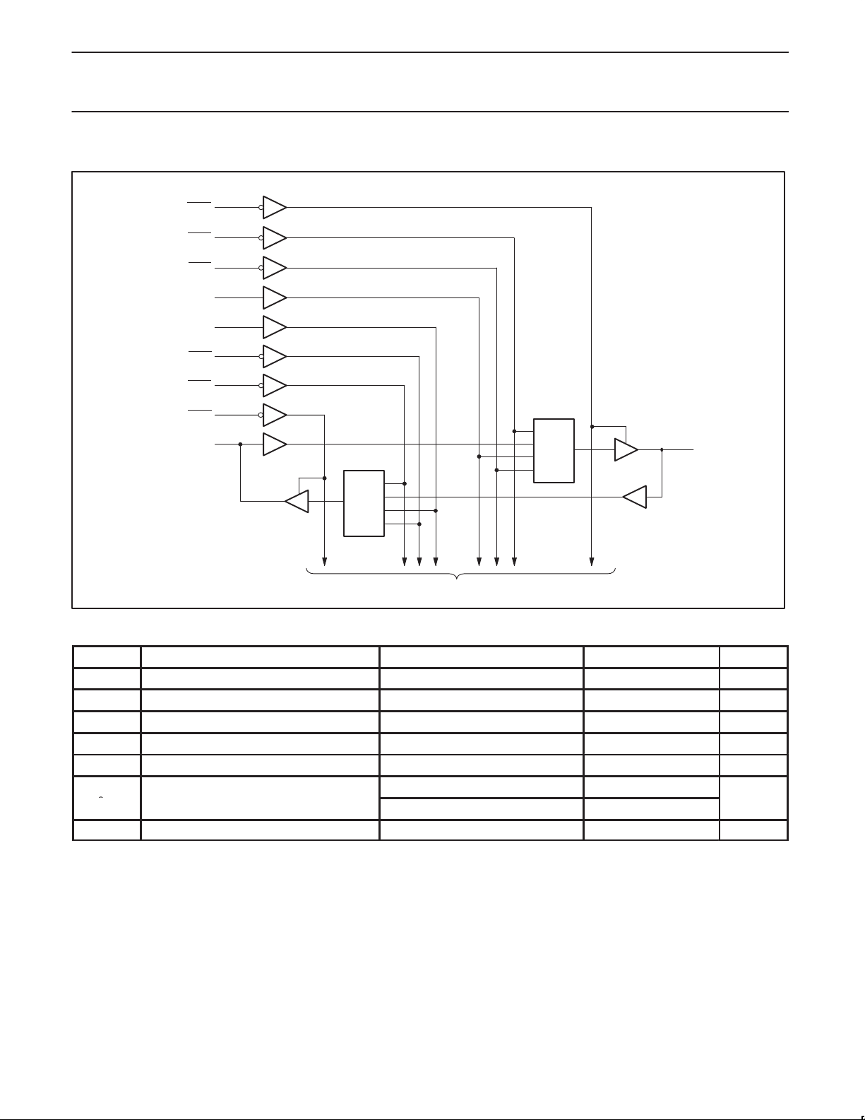
FUNCTION TABLE
INPUTS OUTPUT
CEAB OEAB LEAB CPAB A B
X H X X X Z
X L H X L L
X L H X H H
H L L X X
L L L ↓ L L
L L L ↓ H H
L L L H X
L L L L X B
X =Don’t care
H =High voltage level
L =Low voltage level
↓ =High-to-Low clock transition
† A-to-B data flow is shown: B-to-A flow is similar but uses OEBA
LEBA, CPBA
Output level before the indicated steady-state input conditions
, and CEBA.
were established.
§ Output level before the indicated steady-state input conditions
were established, provided that CLKAB was Low before LEAB
went Low.
B
O
B
O
§
O
,
PIN CONFIGURATION
74ALVT16600
1
OEAB
2
LEAB
A0
3
4
GND
5
A1
6
A2
7
V
CC
8
A3
9
A4
10
A5
11
GND
12
A6
13
A7
14
A8
15
A9
16
A10
17
A11
18
GND GND
19
A12
20
A13
21
A14
22
V
CC
23
A15
24
A16
25
GND
26
A17
27
OEBA
28 29
LEBA
56
55
54
53
52
51
50
49
48
47
46
45
44
43
42
41
40
39
38
37
36
35
34
33
32
31
30
SW00191
CEAB
CPAB
B0
GND
B1
B2
V
CC
B3
B4
B5
GND
B6
B7
B8
B9
B10
B11
B12
B13
B14
V
CC
B15
B16
GND
B17
CPBA
CEBA
1998 Feb 13
3
Philips Semiconductors Product specification
I
DC output current
mA
2.5V/3.3V 18-bit universal bus transceiver (3-State)
LOGIC DIAGRAM (Positive Logic)
1
OEAB
56
CEAB
55
CPAB
2
LEAB
28
LEBA
30
CPBA
29
CEBA
27
OEBA
3
A0
CE
ID
C1
CLK
CE
ID
C1
CLK
74ALVT16600
54
B0
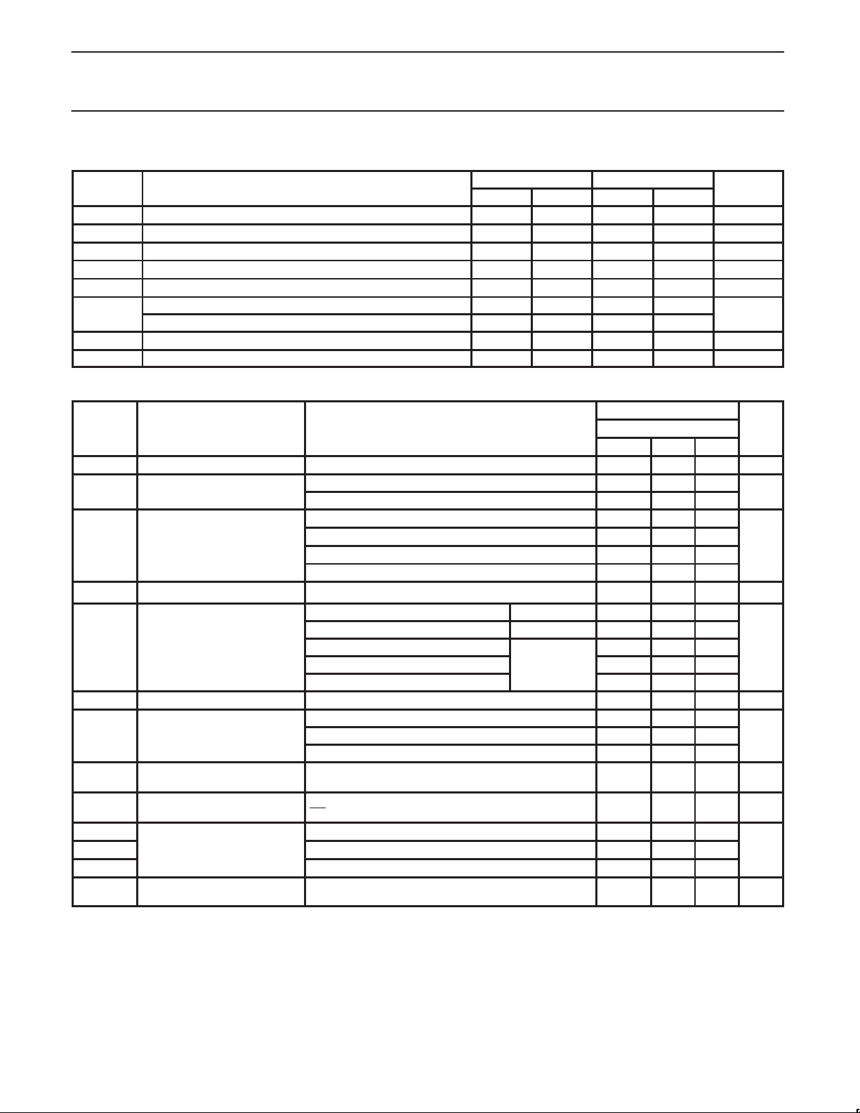
ABSOLUTE MAXIMUM RATINGS
SYMBOL
V
CC
I
IK
V
I
I
OK
V
OUT
OUT
T
stg
DC supply voltage –0.5 to +4.6 V
DC input diode current VI < 0 –50 mA
DC input voltage
DC output diode current VO < 0 –50 mA
DC output voltage
p
Storage temperature range –65 to +150 °C
PARAMETER CONDITIONS RATING UNIT
3
3
To 17 other channels
1, 2
–0.5 to +7.0 V
Output in Off or High state –0.5 to +7.0 V
Output in Low state 128
Output in High state –64
SW00190
NOTES:
1. Stresses beyond those listed may cause permanent damage to the device. These are stress ratings only and functional operation of the
device at these or any other conditions beyond those indicated under “recommended operating conditions” is not implied. Exposure to
absolute-maximum-rated conditions for extended periods may affect device reliability .
2. The performance capability of a high-performance integrated circuit in conjunction with its thermal environment can create junction
temperatures which are detrimental to reliability. The maximum junction temperature of this integrated circuit should not exceed 150°C.
3. The input and output negative voltage ratings may be exceeded if the input and output clamp current ratings are observed.
1998 Feb 13
4
Philips Semiconductors Product specification
SYMBOL
PARAMETER
UNIT
I
mA
VOHHigh-level out ut voltage
V
4
Bus Hold current
Data inputs
7
2.5V/3.3V 18-bit universal bus transceiver (3-State)
74ALVT16600
RECOMMENDED OPERATING CONDITIONS
2.5V RANGE LIMITS 3.3V RANGE LIMITS
MIN MAX MIN MAX
V
CC
V
V
V
I
OH
OL
DC supply voltage 2.3 2.7 3.0 3.6 V
Input voltage 0 5.5 0 5.5 V
I
High-level input voltage 1.7 2.0 V
IH
Input voltage 0.7 0.8 V
IL
High-level output current –8 –32 mA
Low-level output current 8 32
Low-level output current; current duty cycle ≤ 50%; f ≥ 1kHz 24 64
∆t/∆v Input transition rise or fall rate; Outputs enabled 10 10 ns/V
T
amb
Operating free-air temperature range –40 +85 –40 +85 °C
DC ELECTRICAL CHARACTERISTICS (3.3V 0.3V RANGE)
LIMITS
SYMBOL PARAMETER TEST CONDITIONS Temp = -40°C to +85°C UNIT
MIN TYP1MAX
V
V
V
RST
I
OFF
I
HOLD
I
EX
I
PU/PD
I
CCH
I
CCL
I
CCZ
∆I
NOTES:
1. All typical values are at V
2. This is the increase in supply current for each input at the specified voltage level other than V
3. This parameter is valid for any V
transition time of 100µsec is permitted. This parameter is valid for T
4. Unused pins at V
5. I
CCZ
6. For valid test results, data must not be loaded into the flip-flops (or latches) after applying power.
7. This is the bus hold overdrive current required to force the input to the opposite logic state.
Input clamp voltage VCC = 3.0V; IIK = –18mA –0.85 –1.2 V
IK
p
VCC = 3.0 to 3.6V; IOH = –100µA VCC–0.2 V
VCC = 3.0V; IOH = –32mA 2.0 2.3
CC
VCC = 3.0V; IOL = 100µA 0.07 0.2
Low–level output voltage VCC = 3.0V; IOL = 16mA 0.25 0.4 V
OL
VCC = 3.0V; IOL = 32mA 0.3 0.5
VCC = 3.0V; IOL = 64mA 0.4 0.55
Power-up output low voltage6VCC = 3.6V; IO = 1mA; VI = VCC or GND 0.55 V
VCC = 3.6V; VI = VCC or GND Control pins 0.1 ±1
VCC = 0 or 3.6V; VI = 5.5V 0.1 10
I
Input leakage current
I
VCC = 3.6V; VI = 5.5V
VCC = 3.6V; VI = V
CC
Data pins
0.1 20
0.5 10
VCC = 3.6V; VI = 0V 0.1 -5
Off current VCC = 0V; VI or VO = 0 to 4.5V 0.1 ±100 µA
VCC = 3V; VI = 0.8V 75 130
p
Current into an output in the
High state when VO > V
Power up/down 3-State output
3
current
CC
Quiescent supply current VCC = 3.6V; Outputs Low, VI = GND or V
Additional supply current per
CC
input pin
is measured with outputs pulled up to VCC or pulled down to ground.
2
or GND.
CC
= 3.3V and T
CC
CC
between 0V and 1.2V with a transition time of up to 10msec. From V
VCC = 3V; VI = 2.0V –75 –140
VCC = 0V to 3.6V; VCC = 3.6V ±500
VO = 5.5V; VCC = 3.0V 10 125 µA
VCC ≤ 1.2V; VO = 0.5V to VCC; VI = GND or VCC
OE = Don’t care
VCC = 3.6V; Outputs High, VI = GND or V
CC,
VCC = 3.6V; Outputs Disabled; VI = GND or V
VCC = 3V to 3.6V; One input at VCC–0.6V,
Other inputs at VCC or GND
= 25°C.
amb
= 25°C only.
amb
I
0 0.06 0.1
CC,
O =
I
0 4.0 5 mA
O =
CC,
I
O =
or GND
CC
5
0
= 1.2V to VCC = 3.3V ± 0.3V a
CC
1.0 ±100 µA
0.06 0.1
0.04 0.4 mA
µA
µA
1998 Feb 13
5
 Loading...