

Philips 74alvt16500 DATASHEETS

INTEGRATED CIRCUITS
74ALVT16500
2.5V/3.3V 18-bit universal bus
transceiver (3-State)
Product specification
Replaces data of 1997 May 12
IC23 Data Handbook
1998 Feb 13
Philips Semiconductors Product specification
SYMBOL
PARAMETER
UNIT
74AL VT165002.5V/3.3V 18-bit universal bus transceiver (3-State)
FEA TURES
•18-bit bidirectional bus interface
•5V I/O Compatible
•3-State buffers
•Output capability: +64mA/-32mA
•TTL input and output switching levels
•Input and output interface capability to systems at 5V supply
•Bus-hold data inputs eliminate the need for external pull-up
resistors to hold unused inputs
•Live insertion/extraction permitted
•Power-up reset
•Power-up 3-State
•No bus current loading when output is tied to 5V bus
•Negative edge-triggered clock inputs
•Latch-up protection exceeds 500mA per JEDEC JC40.2 Std 17
•ESD protection exceeds 2000V per MIL STD 883 Method 3015
and 200V per Machine Model
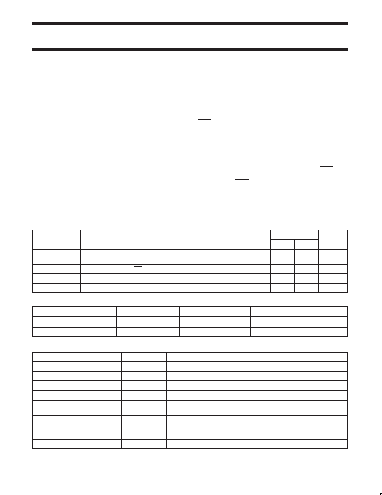
QUICK REFERENCE DATA
t
PLH
t
PHL
C
C
I
CCZ
IN
I/O
Propagation delay
An to Bn or Bn to An
Input capacitance DIR, OE VI = 0V or V
I/O pin capacitance Outputs disabled; V
Total supply current Outputs disabled 40 60 µA
CL = 50pF
DESCRIPTION
The 74ALVT16500 is a high-performance BiCMOS product
designed for V
up to 5V .
This device is an 18-bit universal transceiver featuring non-inverting
3-State bus compatible outputs in both send and receive directions.
Data flow in each direction is controlled by output enable (OEAB and
OEBA
), latch enable (LEAB and LEBA), and clock (CPAB and
) inputs. For A-to-B data flow, the device operates in the
CPBA
transparent mode when LEAB is High. When LEAB is Low, the A
data is latched if CPAB
is Low, the A-bus data is stored in the latch/flip-flop on the
High-to-Low transition of CPAB
are active. When OEAB is Low, the outputs are in the
high-impedance state.
Data flow for B-to-A is similar to that of A-to-B but uses OEBA
LEBA and CPBA
active High, and OEBA
Active bus-hold circuitry is provided to hold unused or floating data
inputs at a valid logic level.
CONDITIONS
T
= 25°C; GND = 0V
amb
CC
operation at 2.5V and 3.3V with I/O compatibility
CC
is held at a High or Low logic level. If LEAB
. When OEAB is High, the outputs
. The output enables are complimentary (OEAB is
is active Low).
TYPICAL
2.5V 3.3V
= 0V or V
I/O
CC
1.9
2.4
4 4 pF
8 8 pF
1.5
1.8
,
ns
ORDERING INFORMATION
PACKAGES TEMPERATURE RANGE OUTSIDE NORTH AMERICA NORTH AMERICA DWG NUMBER
56-Pin Plastic SSOP Type III –40°C to +85°C 74ALVT16500 DL AV16500 DL SOT371-1
56-Pin Plastic TSSOP Type II –40°C to +85°C 74ALVT16500 DGG AV16500 DGG SOT364-1
PIN DESCRIPTION
PIN NUMBER SYMBOL NAME AND FUNCTION
1 OEAB A-to-B Output enable input
27 OEBA B-to-A Output enable input (active low)
2, 28 LEAB/LEBA A-to-B/B-to-A Latch enable input
55,30 CPAB/CPBA A-to-B/B-to-A Clock input (active falling edge)
3, 5, 6, 8, 9, 10, 12, 13, 14, 15,
16, 17, 19, 20, 21, 23, 24, 26
54, 52, 51, 49, 48, 47, 45, 44, 43,
42, 41, 40, 38, 37, 36, 34, 33, 31
4, 11, 18, 25, 29, 32, 39, 46, 53, 56 GND Ground (0V)
7, 22, 35, 50 V
1998 Feb 13 853-1980 18959
A0-A17 Data inputs/outputs (A side)
B0-B17 Data inputs/outputs (B side)
CC
Positive supply voltage
2

Philips Semiconductors Product specification
2.5V/3.3V 18-bit universal bus transceiver (3-State)
PIN CONFIGURA TION
OEAB
1
LEAB
2
3
A0
4
GND
5
A1
6
A2
7
V
CC
8
A3
9
A4
10
A5
11
GND
12
A6
13
A7
14
A8
15
A9
16
A10
17
A11
18
GND GND
19
A12
20
A13
21
A14
22
V
CC
23
A15
24
A16
25
GND
26
A17
27
OEBA
28 29
LEBA
GND
56
CPAB
55
54
B0
GND
53
52
B1
51
B2
50
V
CC
49
B3
48
B4
47
B5
46
GND
45
B6
44
B7
43
B8
42
B9
41
B10
40
B11
39
38
B12
37
B13
36
B14
35
V
CC
34
B15
33
B16
32
GND
31
B17
30
CPBA
GND
LOGIC SYMBOL (IEEE/IEC)
74ALVT16500
1
55
2
27
30
28
3
5
6
8
9
10
12
13
14
15
16
17
19
20
21
23
24
26
EN1
2C3
C3
G2
EN4
5C6
C6
G5
3D 1 1
416D
54
52
51
49
48
47
45
44
43
42
41
40
38
37
36
34
33
31
LOGIC SYMBOL
54
52
51
49
48
47
45
44
43
42
41
40
38
37
36
34
33
31
1998 Feb 13
B0
B1
B2
B3
B4
B5
B6
B7
B8
B9
B10
B11
B12
B13
B14
B15
B16
B17
CPBA
LEBA
OEBA
CPAB
SW00035
LEAB
1255272830
OEAB
A10
A11
A12
A13
A14
A15
A16
A17
A0
A1
A2
A3
A4
A5
A6
A7
A8
A9
SW00036
3
5
6
8
9
10
12
13
14
15
16
17
19
20
21
23
24
26
SW00034
3
Philips Semiconductors Product specification
Disabled, Latch data
Disabled, Clock data
Transparent
Latch data & displa
Clock data & displa
Hold data & displa
2.5V/3.3V 18-bit universal bus transceiver (3-State)
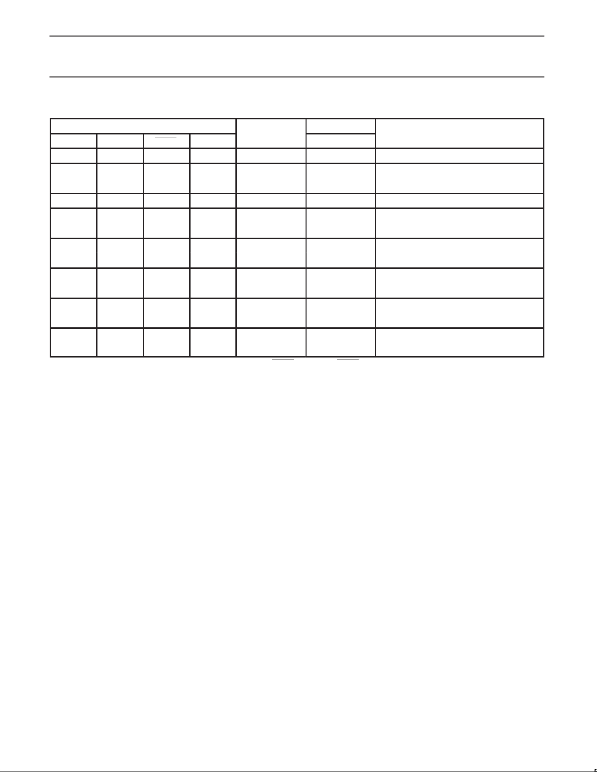
FUNCTION TABLE
INPUTS
OEAB LEAB CPAB An
L H X X X Z Disabled
L ↓ X h H Z
L ↓ X I L Z
L L H or L X NC Z Disabled, Hold data
L L ↓ h H Z
L L ↓ I L Z
H H X H H H
H H X L L L
H ↓ X h H H
H ↓ X I L L
H L ↓ h H H
H L ↓ I L L
H L H or L X H H
H L H or L X L L
NOTE: A-to-B data flow is shown; B-to-A flow is similar but uses OEBA, LEBA, and CPBA.
H = High voltage level
h = High voltage level one set-up time prior to the Enable or Clock transition
L = Low voltage level
I = Low voltage level one set-up time prior to the Enable or Clock transition
NC= No Change
X = Don’t care
Z = High Impedance ”off” state
↓ = High-to-Low Enable or Clock transition
Internal
Registers
OUTPUTS
Bn
OPERATING MODE
74ALVT16500
p
p
y
p
y
p
y
1998 Feb 13
4
Philips Semiconductors Product specification
2.5V/3.3V 18-bit universal bus transceiver (3-State)
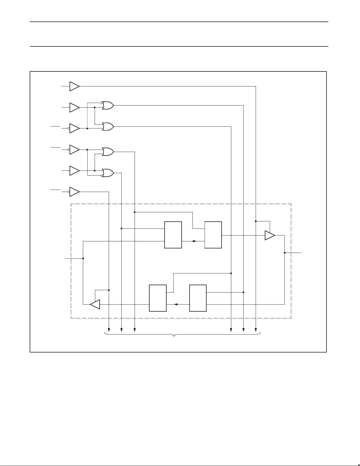
LOGIC DIAGRAM
1
OEAB
28
LEBA
30
CPBA
55
CPAB
2
LEAB
27
OEBA
74ALVT16500
AO
C1
ID
3
1 of 18 channels
C1
ID
To 17 other channels
C1
ID
54
B0
C1
ID
SW00037
1998 Feb 13
5
 Loading...