

Philips 74alvt16374 DATASHEETS
INTEGRATED CIRCUITS
74ALVT16374
2.5V/3.3V 16-bit edge-triggered
D-type flip-flop (3-State)
Product specification
Supersedes data of 1998 Feb 13
IC23 Data Handbook
1999 Oct 18
Philips Semiconductors Product specification
SYMBOL
PARAMETER
UNIT
2.5V/3.3V 16-bit edge-triggered D-type flip-flop
(3-State)
FEA TURES
•16-bit edge-triggered flip-flop
•5V I/O compatibile
•3-State buffers
•Output capability: +64mA/-32mA
•TTL input and output switching levels
•Input and output interface capability to systems at 5V supply
•Bus-hold data inputs eliminate the need for external pull-up
resistors to hold unused inputs
•Live insertion/extraction permitted
•Power-up reset
•Power-up 3-State
•No bus current loading when output is tied to 5V bus
•Latch-up protection exceeds 500mA per JEDEC Std 17
•ESD protection exceeds 2000V per MIL STD 883 Method 3015
and 200V per Machine Model
DESCRIPTION
The 74ALVT16374 is a high-performance BiCMOS product
designed for V
to 5V .
This device is a 16-bit edge-triggered D-type flip-flop featuring
non-inverting 3-State outputs. The device can be used as two 8-bit
flip-flops or one 16-bit flip-flop. On the positive transition of the clock
(CP), the Q outputs of the flip-flop take on the logic levels set up at
the D inputs.
74AL VT16374
operation at 2.5V or 3.3V with I/O compatibility up
CC
QUICK REFERENCE DATA
TYPICAL
2.5V 3.3V
2.6
2.8
3 3 pF
9 9 pF
2.1
2.3
t
PLH
t
PHL
C
C
I
CCZ
IN
Out
CONDITIONS
T
= 25°C
amb
Propagation delay
nCP to nQx
Input capacitance DIR, OE VI = 0V or V
Output capacitance Outputs disabled; VO = 0V or V
Total supply current Outputs disabled 40 40 µA
CL = 50pF
CC
CC
ORDERING INFORMATION
PACKAGES TEMPERATURE RANGE OUTSIDE NORTH AMERICA NORTH AMERICA DWG NUMBER
48-Pin Plastic SSOP Type III –40°C to +85°C 74ALVT16374 DL AV16374 DL SOT370-1
48-Pin Plastic TSSOP Type II –40°C to +85°C 74ALVT16374 DGG AV16374 DGG SOT362-1
ns
1999 Oct 18 853-1844 22537
2
Philips Semiconductors Product specification
2.5V/3.3V 16-bit edge-triggered D-type flip-flop
(3-State)
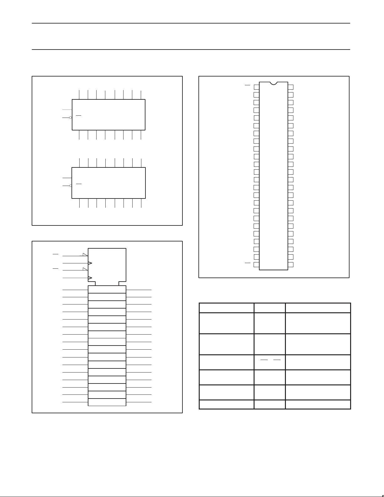
LOGIC SYMBOL
47 46 44 43
1
1D0 1D1 1D2 1D3
1CP
1OE
1Q0 1Q1 1Q2651Q3
32
36 35 33 32
2D02D21 2D2 2D3
2CP
2OE
2Q0 2Q1 2Q2 2Q3
1413 1716
48
25
24
LOGIC SYMBOL (IEEE/IEC)
1OE
1CP
2OE
2CP
1D1
1D2
1D3
1D4
1D5
1D6
1D7
1D8
2D1
2D2
2D3
2D4
2D5
2D6
2D7
2D8
1
48
24
25
47
46
44
43
41
40
38
37
36
35
33
32
30
29
27
26
1EN
C1
2EN
C2
1D
2D
41 40 38 37
1D4 1D5 1D6 1D7
1Q4 1Q5 1Q6
30 29 27 26
2D4 2D5 2D6 2D7
2Q4 2Q5 2Q6 2Q7
98
2019 2322
1 ∇
2 ∇
1Q7
1211
SW00018
2
1Q1
3
1Q2
5
1Q3
6
1Q4
8
1Q5
9
1Q6
11
1Q7
12
1Q8
13
2Q1
14
2Q2
16
2Q3
17
2Q4
19
2Q5
20
2Q6
22
2Q7
23
2Q8
SW00016
PIN CONFIGURATION
PIN DESCRIPTION
47, 46, 44, 43, 41, 40,
38, 37 36, 35, 33, 32,
2, 3, 5, 6, 8, 9, 11, 12
13, 14, 16, 17, 19, 20,
4, 10, 15, 21, 28, 34,
74ALVT16374
1
1OE
1Q0
2
!Q1
3
GND
4
1Q2
5
1Q3
6
V
7
CC
1Q4
8
1Q5
9
GND
10
1Q6
11
1Q7
12
2Q0
13
2Q1
14
GND
15
2Q2
16
2Q3
17
V
18
CC
2Q4
19
2Q5
20
GND
21
2Q6
22
2Q7
23
2OE
24
SW00017
PIN NUMBER SYMBOL FUNCTION
1D0 - 1D7
30, 29, 27, 26
2D0 - 2D7
1Q0 - 1Q7
22, 23
2Q0 - 2Q7
1, 24 1OE, 2OE
48, 25 1CP, 2CP
39, 45
7, 18, 31, 42 V
GND Ground (0V)
CC
1CP
48
1D0
47
1D1
46
GND
45
1D2
44
1D3
43
V
42
CC
1D4
41
1D5
40
GND
39
1D6
38
1D7
37
2D0
36
2D1
35
GND
34
2D2
33
2D3
32
V
31
CC
2D4
30
2D5
29
GND
28
2D6
27
2D7
26
2CP
25
Data inputs
Data outputs
Output enable inputs
(active-Low)
Clock pulse inputs (active
rising edge)
Positive supply voltage
1999 Oct 18
3
Philips Semiconductors Product specification
OPERATING MODE
2.5V/3.3V 16-bit edge-triggered D-type flip-flop
(3-State)
FUNCTION TABLE
INPUTS INTERNAL OUTPUTS
nOE nCP nDx REGISTER nQ0 - nQ7
L
L
L ↑ X NC NC Hold
H
H
H = High voltage level
h = High voltage level one set-up time prior to the High-to-Low E transition
L = Low voltage level
l = Low voltage level one set-up time prior to the High-to-Low E transition
NC= No change
X = Don’t care
Z = High impedance “off” state
↑ = Low-to-High clock transition
= Not a Low-to-High clock transition
↑
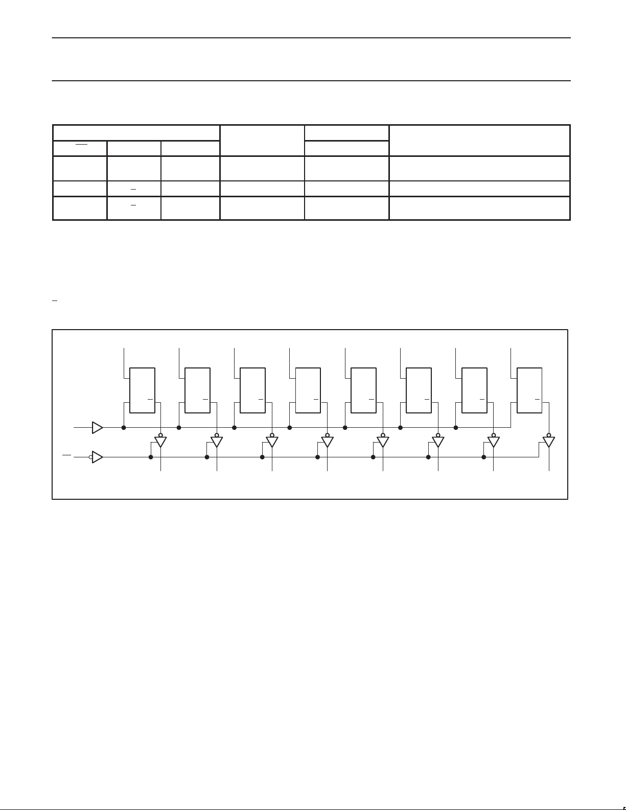
LOGIC DIAGRAM
nD0
↑
↑
↑
↑
nD1
h
X
nDx
l
nD2
L
H
NC
nDx
nD3
L
H
Z
Z
nD4
Load and read register
Disable outputs
nD5
nD6
74ALVT16374
nD7
nCP
nOE
D
CP Q
nQ0
D
CP Q
nQ1 nQ2 nQ3 nQ4 nQ5 nQ6 nQ7
D
CP Q
D
CP Q
D
CP Q
D
CP Q
D
CP Q
D
CP Q
SW00019
1999 Oct 18
4
 Loading...