

Philips 74ALVT162827DL, 74ALVT162827DGG Datasheet

INTEGRATED CIRCUITS
74ALVT162827
20-bit buffer/line driver, non-inverting,
with 30Ω termination resistors (3-State)
Product specification
Supersedes data of 1997 May 01
IC23 Data Handbook
1998 Feb 13
Philips Semiconductors Product specification
SYMBOL
PARAMETER
UNIT
2.5V/3.3V 20-bit buffer/line driver, non-inverting,
with 30Ω termination resistors (3-State)
FEA TURES
•Multiple V
and GND pins minimize switching noise
CC
•5V I/O Compatible
•Live insertion/extraction permitted
•3-State output buffers
•Outputs include series resistance of 30Ω making external
termination resistors unnecessary
•Power-up 3-State
•Output capability: +12mA/–12mA
•Latch-up protection exceeds 500mA per Jedec Std 17
•ESD protection exceeds 2000 V per MIL STD 883 Method 3015
and 200 V per Machine Model
•Bus hold data inputs eliminate the need for external pull-up
resistors to hold unused inputs
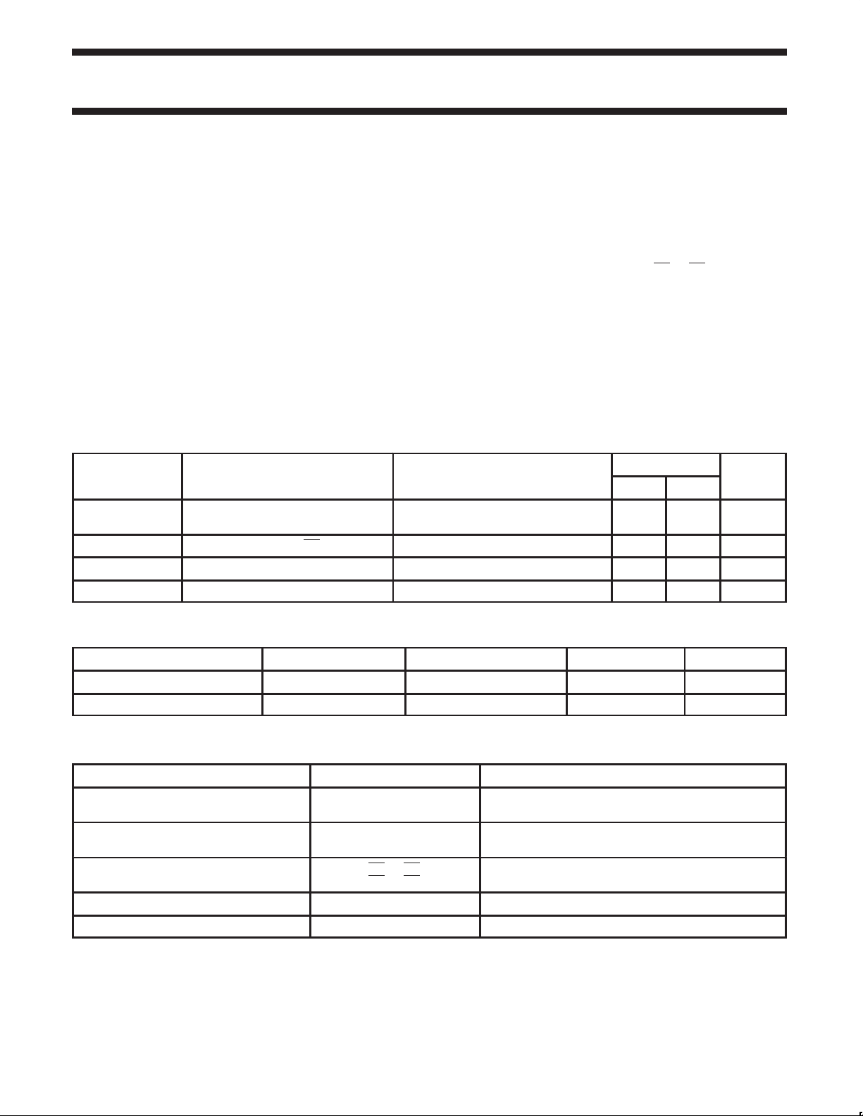
QUICK REFERENCE DATA
t
PLH
t
PHL
C
C
I
CCZ
IN
Out
Propagation delay
nAx to nBx or nBx to nAx
Input capacitance DIR, OE VI = 0V or V
Output capacitance V
Total supply current Outputs disabled 40 70 µA
CL = 50pF
DESCRIPTION
The 74ALVT162827 high-performance BiCMOS device combines
low static and dynamic power dissipation with high speed and high
output drive. It is designed for V
compatibility to 5V .
The 74ALVT162827 20-bit buffers provide high performance bus
interface buffering for wide data/address paths or buses carrying
parity. They have NOR Output Enables (nOE
control flexibility.
The 74ALVT162827 is designed with 30Ω series resistance in both
the pull-up and pull-down output structures. This design reduces line
noise in applications such as memory address drivers, clock drivers
and bus receivers/transmitters.
CONDITIONS
T
amb
CC
= 0V or V
I/O
CC
= 25°C
74ALVT162827
operation at 2.5V or 3.3V with I/O
CC
1, nOE2) for maximum
TYPICAL
2.5V 3.3V
2.7
2.3
3 3 pF
9 9 pF
2.2
2.0
ns
ORDERING INFORMATION
PACKAGES TEMPERATURE RANGE OUTSIDE NORTH AMERICA NORTH AMERICA DWG NUMBER
56-Pin Plastic SSOP Type III –40°C to +85°C 74ALVT162827 DL AV162827 DL SOT371-1
56-Pin Plastic TSSOP Type II –40°C to +85°C 74ALVT162827 DGG AV162827 DGG SOT364-1
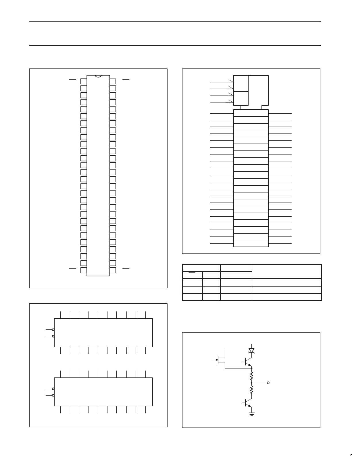
PIN DESCRIPTION
PIN NUMBER SYMBOL FUNCTION
55, 54, 52, 51, 49, 48, 47, 45, 44, 43,
42, 41, 40, 38, 37, 36, 34, 33, 31, 30
2, 3, 5, 6, 8, 9, 10, 12, 13, 14,
15, 16, 17, 19, 20, 21, 23, 24, 26, 27
1, 56,
28, 29
4, 11, 18, 25, 32, 39, 46, 53 GND Ground (0V)
7, 22, 35, 50 V
1A0 - 1A9
2A0 - 2A9
1Y0 - 1Y9
2Y0 - 2Y9
1OE0, 1OE1
2OE0, 2OE1
CC
Data inputs
Data outputs
Output enable inputs (active-Low)
Positive supply voltage
1998 Feb 13 853-1843 18961
2
Philips Semiconductors Product specification
OPERATING MODE
2.5V/3.3V 20-bit buffer/line driver, non-inverting,
with 30Ω termination resistors (3-State)
PIN CONFIGURATION
1
2
1Y0
3
1Y1
4
GND
5
1Y2
6
1Y3
7
V
CC
8
1Y4
9
1Y5
10
1Y6
GND
11
1Y7
12
1Y8
13
1Y9
14
2Y0
15
2Y1
16
2Y2
17
GND
18
2Y3
19
2Y4
20
2Y5
21
V
22
CC
23
2Y6
24
2Y7
25
GND
26
2Y8
27
2Y9
28 29
2OE0
LOGIC SYMBOL
55 54 52 51 49 48 47 45 44 43
1A0 1A1 1A2 1A3 1A4 1A5 1A6 1A7
1
1OE0
56
1OE1
1Y0 1Y1 1Y2 1Y3 1Y4 1Y5 1Y6 1Y7
561OE0
55
54
53
52
51
50
49
48
47
46
45
44
43
42
41
40
39
38
37
36
35
34
33
32
31
30
SH00010
1OE1
1A0
1A1
GND
1A2
1A3
V
CC
1A4
1A5
1A6
GND
1A7
1A8
1A9
2A0
2A1
2A2
GND
2A3
2A4
2A5
V
CC
2A6
2A7
GND
2A8
2A9
2OE1
1A8 1A9
1Y8 1Y9
LOGIC SYMBOL (IEEE/IEC)
FUNCTION TABLE
nOEx nAx nYx
X = Don’t care
Z = High impedance “off” state
H = High voltage level
L = Low voltage level
SCHEMATIC OF EACH OUTPUT
74ALVT162827
1
56
28
29
55
54
52
51
49
48
47
45
44
43
42
41
40
38
37
36
34
33
31
30
INPUTS OUTPUTS
L L L Transparent
L H H Transparent
H X Z High impedance
V
&
EN1
&
EN2
1 ∇
1
2 ∇
1
V
CC
CC
2
3
5
6
8
9
10
12
13
14
15
16
17
19
20
21
23
24
26
27
SH00012
28
29
1998 Feb 13
2 3 5 6 8 9 10 12 13 14
42 41 40 38 37 36 34 33 31 30
2A0 2A1 2A2 2A3 2A4 2A5 2A6 2A7
2OE0
2OE1
2Y0 2Y1 2Y2 2Y3 2Y4 2Y5 2Y6 2Y7
15 16 17 19 20 21 23 24 26 27
2A8 2A9
2Y8 2Y9
SH00011
27Ω
OUTPUT
27Ω
SW00206
3
 Loading...