

Philips 74ALVT162731DL, 74ALVT162731DGG Datasheet

INTEGRATED CIRCUITS
74ALVT162731
2.5V/3.3V 1-to-4 address register/driver
with 30Ω termination resistors (3-State)
Product specification
IC24 Data Handbook
1999 Mar 23
Philips Semiconductors Product specification
SYMBOL
PARAMETER
UNIT
2.5V/3.3V 1-to-4 address register/driver with 30Ω
termination resistors (3-State)
FEA TURES
•5V I/O Compatible
•3-State outputs
•Output capability: +12 mA/-12 mA
•Bus hold data inputs eliminate the need for external pull-up
resistors to hold unused inputs
•Live insertion/extraction permitted
•Power-up reset
•Power-up 3-State
•Positive edge triggered registers
•Latch-up protection exceeds 500 mA per JEDEC JC40.2 Std 17
•ESD protection exceeds 2000 V per MIL STD 883 Method 3015
and 200 V per machine model
•Outputs include series resistance of 30Ω making external
termination resistors unnecessary
•Bus hold data inputs eliminate the need for external pull-up
resistors to hold unused inputs
DESCRIPTION
The 74ALVT162731 is a high-performance BiCMOS product designed
for V
operation at 2.5V to 3.3V with I/O compatibility up to 5V.
CC
This device is a 1-to-4 address register/driver featuring non-inverting
3-State outputs. The state of the outputs are controlled by two
enable inputs (OE1 and OE2). Each enable input controls the state
of two of the four common outputs for each input. When an OEn
input is a logic High, the respective outputs will be in the high
impedance state. When an OEn input is a logic Low, the respective
outputs are active. The device can be configured for a transparent
mode from input to output or a register mode by the SEL input.
When SEL is a logic High the device is configured for transparent
mode and when SEL is a logic Low it is configured for register
mode. While in the register mode the output follows the input on the
rising edge of the CLK input. The function of the data registers is not
effected by either SEL or OEn.
The 74ALVT162731 is designed with 30Ω series resistance in both
the HIGH and LOW states of the output.
74AL VT162731
QUICK REFERENCE DATA
TYPICAL
2.5V 3.3V
3 3 pF
9 9 pF
C
t
PLH
t
PHL
C
OUT
I
CCZ
CONDITIONS
T
= 25°C; GND = 0V
amb
Propagation delay
nAx to nYx
IN
Input capacitance VI = 0V or V
Output capacitance Outputs disabled; VO = 0V or V
Total supply current Outputs disabled 40 60 µA
CL = 50pF 3.8 3.2 ns
CC
CC
ORDERING INFORMATION
PACKAGES TEMPERATURE RANGE OUTSIDE NORTH AMERICA NORTH AMERICA DWG NUMBER
56-Pin Plastic SSOP Type III –40°C to +85°C 74ALVT162731 DL AV162731 DL SOT371-1
56-Pin Plastic TSSOP Type II –40°C to +85°C 74ALVT162731 DGG AV162731 DGG SOT364-1
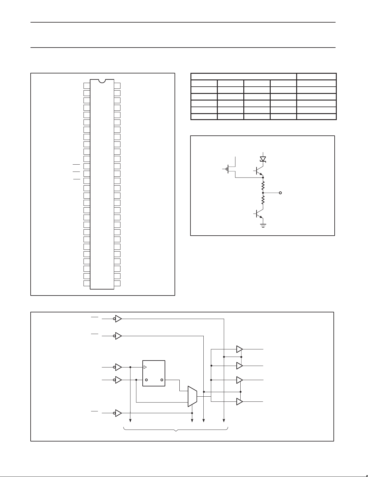
PIN DESCRIPTION
PIN NUMBER SYMBOL NAME AND FUNCTION
1, 4, 19, 25, 28, 32, 38, 41, 47, 53 GND Ground
5, 6, 23, 24, 30, 31, 36, 37, 42, 43,
48, 49, 54, 55
2, 3, 20, 21, 26, 27, 33, 34, 39, 40,
45, 46, 51, 52
7, 22, 29, 35, 44, 50, 56 V
8, 9, 10, 15, 16, 17, 18 A
14 SEL Select input, controls mode of device
11 CLK Clock input
12, 13 OE
1Yn, 2Y
3Yn,4Y
CC
n
n
n
n
Output, controlled by OE1
Output, controlled by OE2
Positive power supply
Data inputs
Output enable
1999 Mar 23 853-2146 21078
2
Philips Semiconductors Product specification
2.5V/3.3V 1-to-4 address register/driver with 30Ω
termination resistors (3-State)
PIN CONFIGURA TION
GND
1
2
4Y
1
3Y
3
1
4
GND
5
2Y
1
6
1Y
1
V
7
CC
8
A
1
9
A
2
10
A
3
11
CLK
12
OE1
13
OE2
14
SEL
15
A
4
16
A
5
17
A
6
18
A
7
19
GND
20
4Y
7
21
3Y
7
V
22
CC
23
2Y
7
24
1Y
7
25
GND
26
4Y
6
27
3Y
6
28 29
GND
56
55
54
53
52
51
50
49
48
47
46
45
44
43
42
41
40
39
38
37
36
35
34
33
32
31
30
SV01733
V
CC
1Y
2Y
GND
3Y
4Y
V
CC
1Y
2Y
GND
3Y
4Y
V
CC
1Y
2Y
GND
3Y
4Y
GND
1Y
2Y
V
CC
3Y
4Y
GND
1Y
2Y
V
cc
2
2
2
2
3
3
3
3
4
4
4
4
5
5
5
5
6
6
FUNCTION TABLE
OE SEL CLK A Y
H X X X Z
L H X L L
L H X H H
L L ↑ L L
L L ↑ H H
SCHEMATIC OF EACH OUTPUT
74ALVT162731
INPUTS OUTPUTS
V
V
CC
CC
27Ω
OUTPUT
27Ω
SW00007
LOGIC DIAGRAM
1999 Mar 23
OE1
OE2
CLK
A1
SEL
CLK
To six other channels
1Y1
2Y1
3Y1
4Y1
SV01734
3
Philips Semiconductors Product specification
I
DC out ut current
mA
SYMBOL
PARAMETER
UNIT
2.5V/3.3V 1-to-4 address register/driver with 30Ω
termination resistors (3-State)
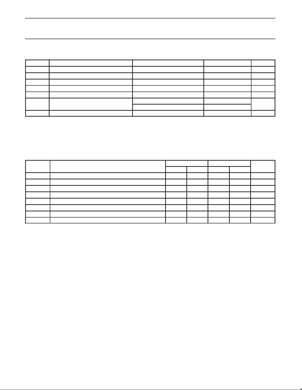
ABSOLUTE MAXIMUM RATINGS
SYMBOL
V
V
I
V
I
OK
OUT
OUT
T
CC
IK
stg
DC supply voltage -0.5 to +4.6 V
DC input diode current VI < 0 -50 mA
DC input voltage
I
DC output diode current VO < 0 -50 mA
DC output voltage
p
Storage temperature range -65 to +150 °C
NOTES:
1. Stresses beyond those listed may cause permanent damage to the device. These are stress ratings only and functional operation of the
device at these or any other conditions beyond those indicated under “recommended operating conditions” is not implied. Exposure to
absolute-maximum-rated conditions for extended periods may affect device reliability .
2. The performance capability of a high-performance integrated circuit in conjunction with its thermal environment can create junction
temperatures which are detrimental to reliability. The maximum junction temperature of this integrated circuit should not exceed 150°C.
3. The input and output negative voltage ratings may be exceeded if the input and output clamp current ratings are observed.
PARAMETER CONDITIONS RATING UNIT
3
3
RECOMMENDED OPERATING CONDITIONS
V
CC
V
V
V
I
OH
I
OL
∆τ/∆ϖ Input transition rise or fall rate; Outputs enabled 10 10 ns/V
T
amb
DC supply voltage 2.3 2.7 3.0 3.6 V
Input voltage 0 5.5 0 5.5 V
I
High-level input voltage 1.7 2.0 V
IH
Input voltage 0.7 0.8 V
IL
High-level output current –8 –12 mA
Low-level output current 8 12 mA
Operating free-air temperature range –40 +85 –40 +85 °C
1, 2
Output in Off or High state -0.5 to +7.0 V
Output in Low state 128
Output in High state -64
2.5V RANGE LIMITS 3.3V RANGE LIMITS
MIN MAX MIN MAX
74ALVT162731
-0.5 to +7.0 V
1999 Mar 23
4
 Loading...