

Philips 74ALVT16260DL, 74ALVT16260DGG Datasheet

INTEGRATED CIRCUITS
74ALVT16260
12-bit to 24-bit multiplexed D-type latches
(3-State)
Product specification
IC23 Data Handbook
1998 Jan 30
Philips Semiconductors Product specification
SYMBOL
PARAMETER
UNIT
C
pF
ns
2.5V/3.3V 12-bit to 24-bit multiplexed D-type latches
(3-State)
FEATURES
•ESD protection exceeds 2000V per Mil-Std-883C, Method 3015;
exceeds 200V using machine model
•Latch-up protection exceeds 500mA per JEDEC Standard
JESD-17.
•Distributed V
switching noise.
•Output capability (–32mA I
and GND pin configuration minimizes high-speed
CC
, 64mA IOL).
OH
•Bus hold inputs eliminate the need for external pull-up resistors.
•5V I/O compatible
•Live insertion/extraction permitted
•Power-up 3-State
•Power-up Reset
DESCRIPTION
The 74ALVT16260 is a 12-bit to 24-bit multiplexed D-type latch used
in applications where two separate data paths must be multiplexed
onto, or demultiplexed from, a single data path. Typical applications
include multiplexing and/or demultiplexing of address and data
information in microprocessor or bus-interface applications. This
device is alto useful in memory-interleaving applications.
Three 12-bit I/O ports (A1–A12, 1B1–1B12, and 2B1–2B12) are
available for address and/or data transfer. The output enable (OE1B
OE2B
, and OEA) inputs control the bus transceiver functions. The
and OE2B control signals also allow bank control in the A to
OE1B
B direction.
Address and/or data information can be stored using the internal
storage latches. The latch enable (LE1B, LE2B, LEA1B, and
LEA2B) inputs are used to control data storage. When the latch
enable input is high, the latch is transparent. When the latch enable
input goes low, the data present at the inputs is latched and remains
latched until the latch enable input is returned high.
To ensure the high-impedance state during power-up or
power-down, OE
the minimum value of the resistor is determined by the current
sinking capability of the driver.
The 74ALVT16260 is available in a 56-pin Shrink Small Outline
Package (SSOP) and 56-pin Thin Shrink Small Outline Package
(TSSOP).
74AL VT16260
,
should be tied to VCC through a pull-up resistor;
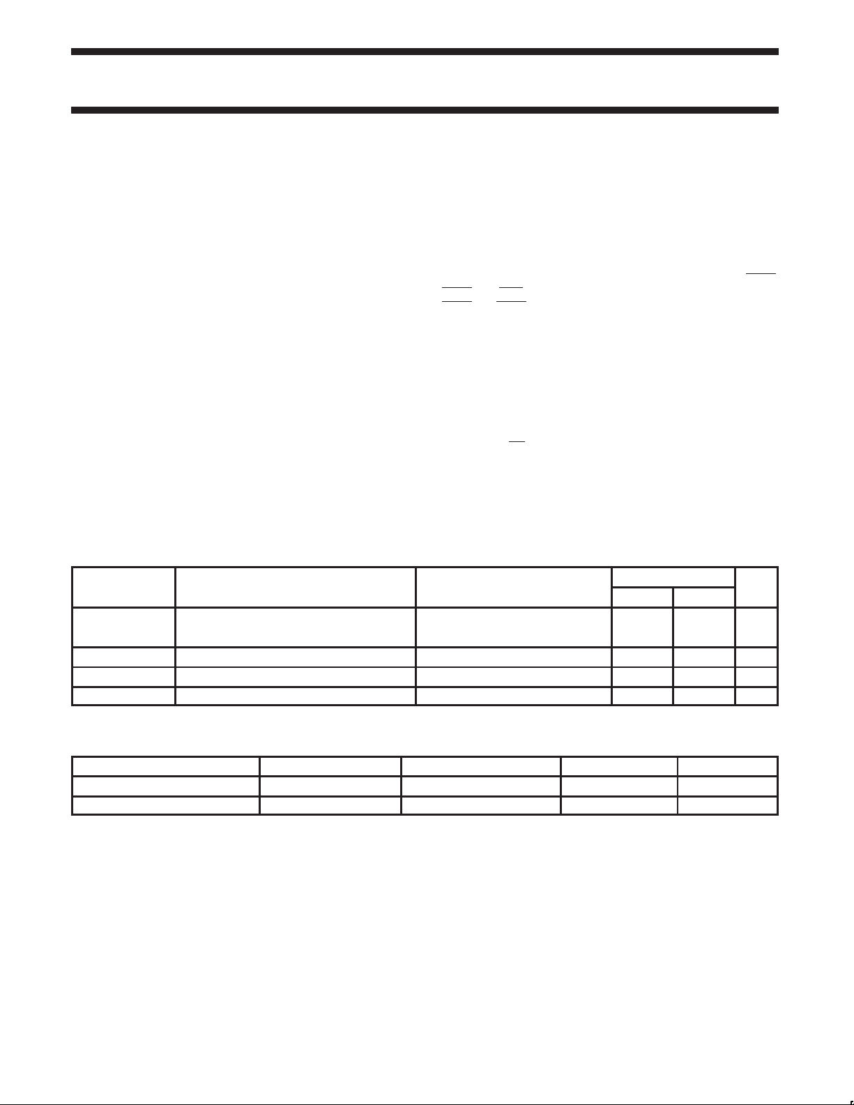
QUICK REFERENCE DATA
TYPICAL
2.5V 3.3V
3.5 2.8
3.3 2.6
4 4 pF
C
t
PLH
t
PHL
C
OUT
I
CCZ
CONDITIONS
T
= 25°C; GND = 0V
amb
Propagation delay
nAx to nBx nBx to nAx
IN
Input capacitance VI = 0 V or V
Output capacitance V
Total supply current Outputs disabled 100 80 µA
I/O
p
= 50
L
CC
= 0 V or 5.0 V 9 9 pF
ORDERING INFORMATION
PACKAGES TEMPERATURE RANGE OUTSIDE NORTH AMERICA NORTH AMERICA DWG NUMBER
56-Pin Plastic SSOP Type III –40°C to +85°C 74ALVT16260 DL AV16260 DL SOT371-1
56-Pin Plastic TSSOP Type II –40°C to +85°C 74ALVT16260 DGG AV16260 DGG SOT364-1
1998 Jan 30 853-2046-18918
2
Philips Semiconductors Product specification
2.5V/3.3V 12-bit to 24-bit multiplexed D-type latches
(3-State)
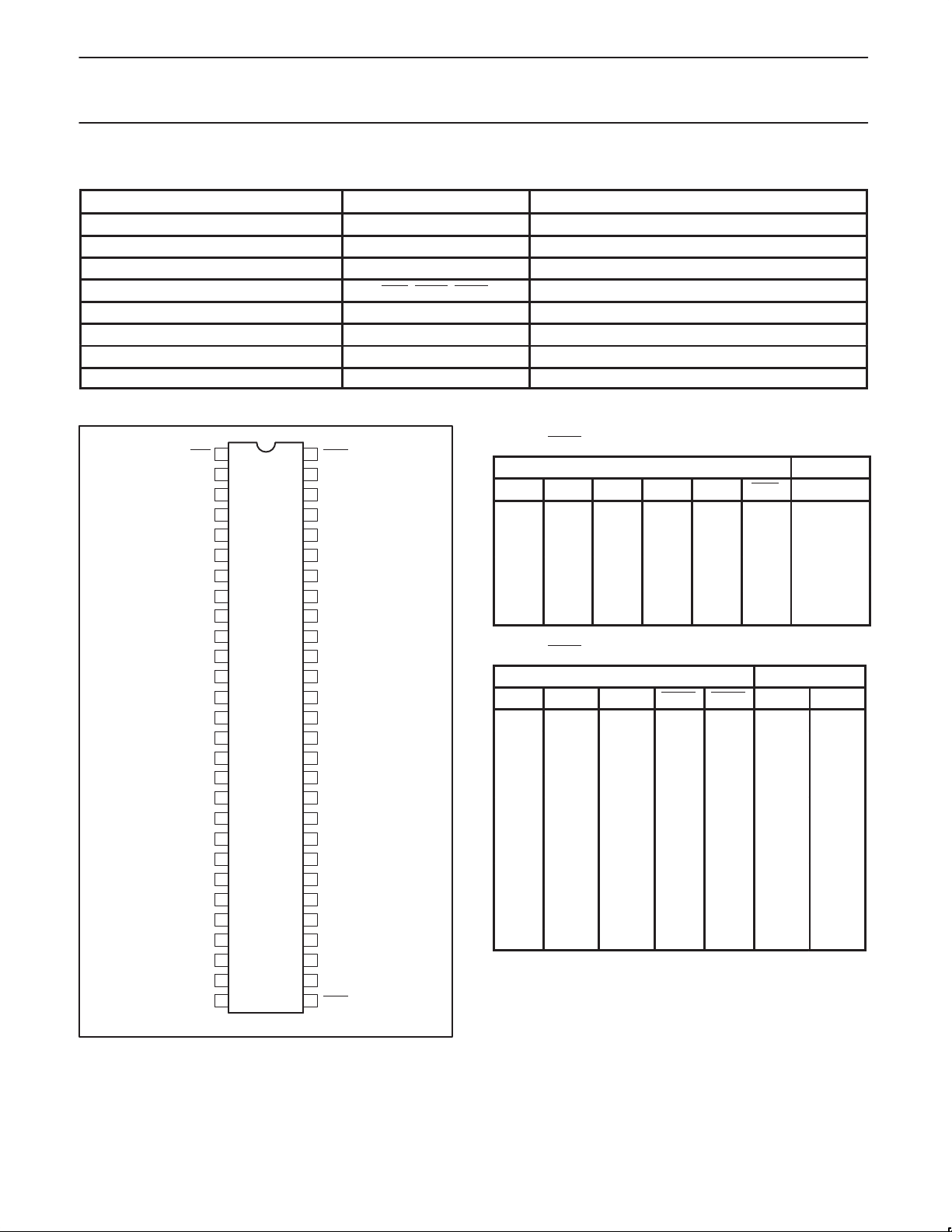
PIN DESCRIPTION
PIN NUMBER SYMBOL FUNCTION
8, 9, 10, 12, 13, 14, 15, 16, 17, 19, 20, 21 An Data inputs/outputs (A)
23, 24, 26, 31, 33, 34, 36, 37, 38, 40, 41, 42 1Bn Data inputs/outputs (B1)
6, 5, 3, 54, 52, 51, 49, 48, 47, 45, 44, 43 2Bn Data inputs/outputs (B2)
1, 29, 56 OEA, OE1B, OE2B Output enable input (active low)
2, 27, 30, 55 LE1B, LE2B, LEA1B, LEA2B Latch enable inputs
28 SEL B1/B2 input select input
4, 11, 18, 25, 32, 39, 46, 53 GND Ground (0V)
7, 22, 35, 50 V
PIN CONFIGURATION
1
2
LE1B
3
2B3
4
GND
5
2B2
6
2B1
7
V
CC
A1
8
A2
9
A3
10
GND
11
12 45
13
A6
14
A7
15
A8
16
A9
17
GND
18 39
19 38
A10
20
21
A12
22
V
CC
23
1B1
24
1B2
25 32
26 31 1B41B3
27 30 LEA1BLE2B
28 29SEL OE1B
CC
FUNCTION TABLES
OE2B
56OEA
55
LEA2B
54
2B4
53
GND
52
2B5
51
2B6
50
V
CC
49
2B7
48
2B8
47
2B9
46
GND
2B10A4
2B11
44A5
2B12
43
1B12
42
1B11
41
1B10
40
GND
1B9
37A11
1B8
36
1B7
35
V
CC
34
1B6
33
1B5
GNDGND
B to A (OEB = H)
A to B (OEA = H)
Positive supply voltage
INPUTS OUTPUT
1B 2B SEL LE1B LE2B OEA A
H X H H X L H
L X H H X L L
X X H L X L A0
X H L X H L H
X L L X H L L
X X L X L L A0
X X X X X H Z
INPUTS OUTPUT
A LEA1B LEA2B OE1B OE2B 1B 2B
H H H L L H H
L H H L L L L
H H L L L H 2B0
L H L L L L 2B0
H L H L L 1B0 H
L L H L L 1B0 L
X L L L L 1B0 2B0
X X X H H Z Z
X X X L H Active Z
X X X H L Z Active
X X X L L Active Active
74ALVT16260
1998 Jan 30
SA00435
3

Philips Semiconductors Product specification
2.5V/3.3V 12-bit to 24-bit multiplexed D-type latches
(3-State)
LOGIC DIAGRAM (POSITIVE LOGIC)
2
LE1B
27
LE2B
30
LEA1B
55
LEA2B
56
OE2B
29
OE1B
1
OEA
28
SEL
G1
8
A1
1
1
74ALVT16260
C1
1D
23
1B1
C1
1D
C1
1D
C1
1D
TO 11 OTHER CHANNELS
6
SA00436
2B1
1998 Jan 30
4

Philips Semiconductors Product specification
I
DC output current
mA
SYMBOL
PARAMETER
UNIT
I
mA
2.5V/3.3V 12-bit to 24-bit multiplexed D-type latches
74ALVT16260
(3-State)
ABSOLUTE MAXIMUM RATINGS
SYMBOL
V
V
I
V
I
OK
OUT
OUT
T
CC
IK
stg
DC supply voltage –0.5 to +4.6 V
DC input diode current VI < 0 –50 mA
DC input voltage
I
DC output diode current VO < 0 –50 mA
DC output voltage
p
Storage temperature range –65 to +150 °C
NOTES:
1. Stresses beyond those listed may cause permanent damage to the device. These are stress ratings only and functional operation of the
device at these or any other conditions beyond those indicated under “recommended operating conditions” is not implied. Exposure to
absolute-maximum-rated conditions for extended periods may affect device reliability .
2. The performance capability of a high-performance integrated circuit in conjunction with its thermal environment can create junction
temperatures which are detrimental to reliability. The maximum junction temperature of this integrated circuit should not exceed 150°C.
3. The input and output negative voltage ratings may be exceeded if the input and output clamp current ratings are observed.
PARAMETER CONDITIONS RATING UNIT
3
3
1, 2
–0.5 to +7.0 V
Output in Off or High state –0.5 to +7.0 V
Output in Low state 128
Output in High state –64
RECOMMENDED OPERATING CONDITIONS
2.5V RANGE LIMITS 3.3V RANGE LIMITS
MIN MAX MIN MAX
V
CC
V
V
V
I
OH
OL
∆t/∆v Input transition rise or fall rate; Outputs enabled 10 10 ns/V
T
amb
DC supply voltage 2.3 2.7 3.0 3.6 V
Input voltage 0 5.5 0 5.5 V
I
High-level input voltage 1.7 2.0 V
IH
Input voltage 0.7 0.8 V
IL
High-level output current –8 –32 mA
Low-level output current 8 32
Low-level output current; current duty cycle ≤ 50%; f ≥ 1kHz 24 64
Operating free-air temperature range –40 +85 –40 +85 °C
1998 Jan 30
5
 Loading...