

Philips 74alvt16240 DATASHEETS

INTEGRATED CIRCUITS
74ALVT16240
16-bit inverting buffer/driver (3-State)
Product specification
Replaces data sheet of 1997 May 02
IC23 Data Handbook
1998 Feb 13
Philips Semiconductors Product specification
SYMBOL
PARAMETER
UNIT
74AL VT162402.5V/3.3V 16-bit inverting buffer/driver (3-State)
FEA TURES
•16-bit bus interface
•5V I/O compatibile
•3-State buffers
•Output capability: +64mA/-32mA
•TTL input and output switching levels
DESCRIPTION
The 74ALVT16240 is a high-performance BiCMOS product
designed for V
to 5V .
This device is an inverting 16-bit buffer that is ideal for driving bus
lines. The device features four Output Enables (1OE
), each controlling four of the 3-State outputs.
4OE
operation at 2.5V or 3.3V with I/O compatibility up
CC
, 2OE, 3OE,
•Input and output interface capability to systems at 5V supply
•Bus-hold data inputs eliminate the need for external pull-up
resistors to hold unused inputs
•Live insertion/extraction permitted
•Power-up 3-State
•No bus current loading when output is tied to 5V bus
•Latch-up protection exceeds 500mA per JEDEC Std 17
•ESD protection exceeds 2000V per MIL STD 883 Method 3015
and 200V per Machine Model
QUICK REFERENCE DATA
CONDITIONS
T
= 25°C
amb
t
PLH
t
PHL
C
C
I
CCZ
IN
O
Propagation delay
nAx to nYx
Input capacitance nOE VI = 0V or V
Output pin capacitance V
CL = 50pF
= 0V or V
I/O
CC
CC
Total supply current Outputs disabled 40 60 µA
ORDERING INFORMATION
PACKAGES TEMPERATURE RANGE OUTSIDE NORTH AMERICA NORTH AMERICA DWG NUMBER
48-Pin Plastic SSOP Type III –40°C to +85°C 74ALVT16240 DL AV16240 DL SOT370-1
48-Pin Plastic TSSOP Type II –40°C to +85°C 74ALVT16240 DGG AV16240 DGG SOT362-1
TYPICAL
2.5V 3.3V
2.5
1.9
1.7
1.7
3 3 pF
9 9 pF
ns
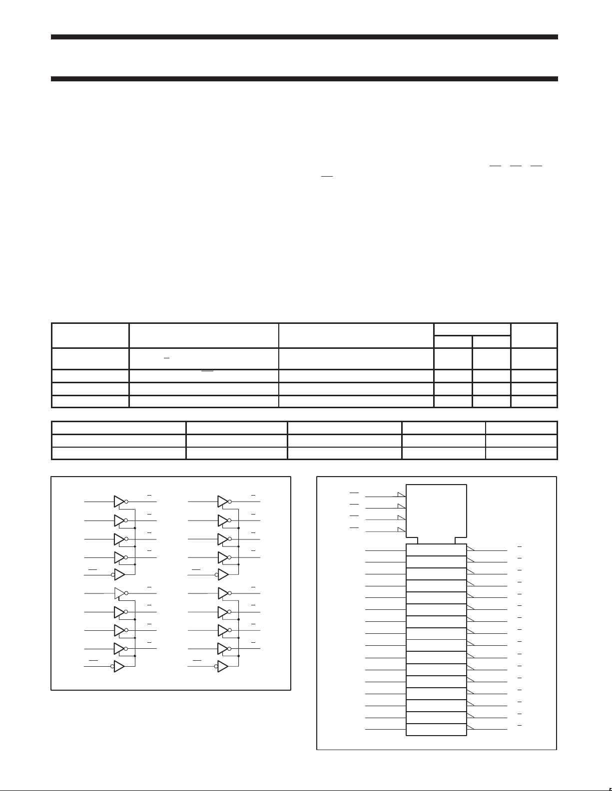
LOGIC SYMBOL
1A0
47
1A1
46
1A2
44
1A3
43
1OE
1
2A0
41
2A1
40
2A2
38
2A3
37
2OE
48
1Y
1Y
1Y
1Y
2Y0
2Y
2Y
2Y
LOGIC SYMBOL (IEEE/IEC)
1
0
1
2
3
1
2
3
3A0
2
36
3A1
35
3
3A2
5
33
3A3
32
6
3OE
25
4A0
8
30
4A1
9
29
4A2
11
27
4A3
12
26
4OE
24
0
3Y
3Y
1
3Y
2
3
3Y
4Y0
4Y
1
2
4Y
4Y
3
SW00004
13
14
16
17
19
20
22
23
1OE
2OE
3OE
4OE
1A1
1A2
1A3
1A4
2A1
2A2
2A3
2A4
3A1
3A2
3A3
3A4
4A1
4A2
4A3
4A4
48
25
24
47
46
44
43
41
40
38
37
36
35
33
32
30
29
27
26
EN1
EN2
EN3
EN4
2
1Y
1
1 ∇
2 ∇1
3 ∇1
4 ∇1
3
1Y
5
1Y
6
1Y
8
2Y
9
2Y
11
2Y
12
2Y
13
3Y
14
3Y
16
3Y
17
3Y
19
4Y
20
4Y2
22
4Y
23
4Y
SW00231
1
2
3
4
1
2
3
4
1
2
3
4
1
3
4
1998 Feb 13 853-1975 18960
2
Philips Semiconductors Product specification
I
DC output current
mA
74ALVT162402.5V/3.3V 16-bit inverting buffer/driver (3-State)
PIN CONFIGURA TION
1
1OE
2
1Y0
1Y
1
3
GND
4
1Y
2
5
3
1Y
6
7
V
CC
8
2Y
0
1
2Y
9
GND
10
2Y
2
11
3
2Y
12
0
3Y
13
3Y
1
14
GND
15
16
3Y2
4
3Y
17
18
V
CC
4Y0
19
20
4Y
1
21
GND
22
4Y2
23
3
4Y
24
4OE
48
47
46
45
44
43
42
41
40
39
38
37
36
35
34
33
32
31
30
29
28
27
26
25
SW00006
2OE
1A0
1A1
GND
1A2
1A3
V
CC
2A0
2A1
GND
2A2
2A3
3A0
3A1
GND
3A2
3A3
V
CC
4A0
4A1
GND
4A2
4A3
3OE
PIN DESCRIPTION
PIN NUMBER SYMBOL NAME AND FUNCTION
47, 46, 44, 43,
41, 40, 38, 37,
36, 35, 33, 32,
30, 29, 27, 26
2, 3, 5, 6,
8, 9, 11, 12,
13, 14, 16, 17,
19, 20, 22, 23
1, 48, 25, 24
4, 10, 15, 21,
28, 34, 39, 45
7, 18, 31, 42 V
1A0-1A3
2A0-2A3
3A0-3A3
Data inputs
4A0-4A3
1Y0-1Y3
2Y
0-2Y3
3Y0-3Y3
Data outputs
4Y0-4Y3
1OE, 2OE,
3OE, 4OE
Output enables
GND Ground (0V)
CC
Positive supply voltage
FUNCTION TABLE
Inputs Outputs
nOE nAx nYx
L L H
L H L
H X Z
H = High voltage level
L = Low voltage level
X = Don’t care
Z = High Impedance “off” state
ABSOLUTE MAXIMUM RATINGS
SYMBOL
V
CC
I
IK
V
I
OK
V
OUT
OUT
T
stg
NOTES:
1. Stresses beyond those listed may cause permanent damage to the device. These are stress ratings only and functional operation of the
DC supply voltage -0.5 to +4.6 V
DC input diode current VI < 0 -50 mA
DC input voltage
I
DC output diode current VO < 0 -50 mA
DC output voltage
p
Storage temperature range -65 to +150 °C
PARAMETER CONDITIONS RATING UNIT
3
3
1, 2
-0.5 to +7.0 V
Output in Off or High state -0.5 to +7.0 V
Output in Low state 128
Output in High state -64
device at these or any other conditions beyond those indicated under “recommended operating conditions” is not implied. Exposure to
absolute-maximum-rated conditions for extended periods may affect device reliability .
2. The performance capability of a high-performance integrated circuit in conjunction with its thermal environment can create junction
temperatures which are detrimental to reliability. The maximum junction temperature of this integrated circuit should not exceed 150°C.
3. The input and output negative voltage ratings may be exceeded if the input and output clamp current ratings are observed.
1998 Feb 13
3
 Loading...