

Philips 74alvch16841 DATASHEETS

INTEGRATED CIRCUITS
74ALVCH16841
20-bit bus interface D-type latch (3-State)
Product specification
IC24 Data Handbook
1998 Jul 27
Philips Semiconductors Product specification
1
CPDPower dissi ation ca acitance er buffer
V
GND to V
1
F
74AL VCH1684120-bit bus interface D-type latch (3-State)
FEA TURES
•Wide supply voltage range of 1.2V to 3.6V
•Complies with JEDEC standard no. 8-1A
•Wide supply voltage range of 1.2V to 3.6V
•CMOS low power consumption
•Direct interface with TTL levels
•MULTIBYTE
•Low inductance multiple V
and ground bounce
TM
flow-through standard pin-out architecture
and GND pins for minimum noise
CC
•Current drive ±24 mA at 3.0 V
•All inputs have bus hold circuitry
•Output drive capability 50Ω transmission lines @ 85°C
•3-State non-inverting outputs for bus oriented applications
DESCRIPTION
The 74ALVCH16841 has two 10-bit D-type latch featuring separate
D-type inputs for each latch and 3-State outputs for bus oriented
applications. The two sections of each register are controlled
independently by the latch enable (nLE) and output enable (nOE)
control gates.
When nOE
When nOE
Operation of the nOE
The 74ALVCH16841 has active bus hold circuitry which is provided
to hold unused or floating data inputs at a valid logic level. This
feature eliminates the need for external pull-up or pull-down
resistors.
is LOW, the data in the registers appears at the outputs.
is High the outputs are in High-impedance OFF state.
input does not affect the state of the flip-flops.
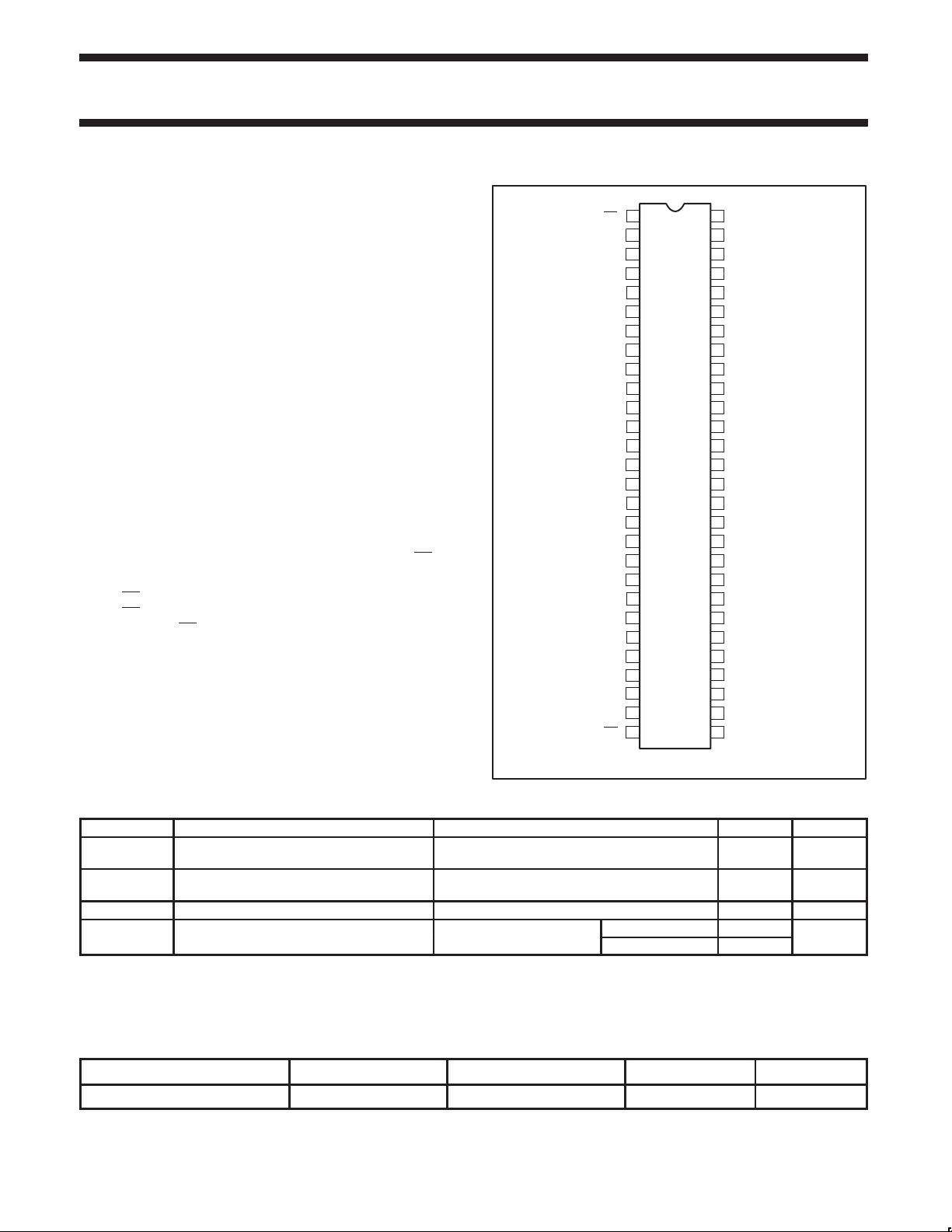
PIN CONFIGURATION
1
1OE
2
1Q0
3
1Q1
4
GND
5
1Q2
6
1Q3
7
V
CC
8
1Q4
9
1Q5
10
1Q6
11
GND
1Q7
12
1Q8
13
14
1Q9
15
2Q0
16
2Q1
17
2Q2
18
GND
2Q3
19
20
2Q4
21
2Q5
22
V
CC
23
2Q6
24
2Q7
GND
25
2Q8
26
2Q9
27
28
2OE
56
1LE
55
1D0
54
1D1
53
GND
1D2
52
1D3
51
50
V
CC
1D4
49
1D5
48
1D6
47
46
GND
1D7
45
1D8
44
1D9
43
2D0
42
2D1
41
2D2
40
GND
39
38
2D3
2D4
37
2D5
36
35
V
CC
34
2D6
33
2D7
32
GND
31
2D8
2D9
30
29
2LE
QUICK REFERENCE DA TA
GND = 0V; T
SYMBOL
t
PHL/tPLH
t
PHL/tPLH
C
I
NOTES:
is used to determine the dynamic power dissipation (PD in µW):
1. C
PD
= CPD × V
P
D
= output frequency in MHz; VCC = supply voltage in V; (CL × V
f
o
= 25°C; tr = tf ≤ 2.5ns
amb
Propagation delay
nDn to nQ
Propagation delay
nLE to nQ
Input capacitance 5.0 pF
2
× fi + (CL × V
CC
ORDERING INFORMATION
PACKAGES TEMPERATURE RANGE OUTSIDE NORTH AMERICA NORTH AMERICA DWG NUMBER
56-Pin Plastic TSSOP Type II –40°C to +85°C 74ALVCH16841 DGG ACH16841 DGG SOT364-1
1998 Jul 27 853-2093 19785
SA00076
PARAMETER CONDITIONS TYPICAL UNIT
VCC = 2.5V, CL = 30pF
n
VCC = 3.3V, CL = 50pF
VCC = 2.5V, CL = 30pF
n
p
p
2
× fo) where: fi = input frequency in MHz; CL = output load capacitance in pF;
CC
p
VCC = 3.3V, CL = 50pF
=
I
CC
CC
2
× fo) = sum of outputs.
Outputs enabled 19
Outputs disabled 3
2.5
2.4
2.5
2.4
2
ns
ns
p
Philips Semiconductors Product specification
74ALVCH1684120-bit bus interface D-type latch (3-State)
PIN DESCRIPTION
PIN NUMBER SYMBOL FUNCTION
1 1OE
56 1LE
55, 54, 52, 51, 49,
48, 47, 45, 44, 43
2, 3, 5, 6, 8, 9, 10,
12, 13, 14
4, 11, 18, 25, 32,
39, 46, 53
7, 22, 35, 50 V
28 2OE
29 2LE
42, 41, 40, 38, 37,
36, 34, 33, 31, 30
15, 16, 17, 19, 20,
21, 23, 24, 26, 27
1D0 – 1D9 Data inputs
1Q0 – 1Q9 Data outputs
GND Ground (0V)
CC
2D0 – 2D9 Data inputs
2Q0 – 2Q9 Data outputs
Output enable inputs
(active-LOW)
Latch enable inputs
(active HIGH)
Positive supply
voltage
Output enable inputs
(active-LOW)
Latch enable inputs
(active HIGH)
FUNCTION TABLE
INPUTS OUTPUT
nOE LE Dx Q
L H L L
L H H H
L L X Q
H X X Z
H = High voltage level
L = Low voltage level
X = Don’t care
Z = High impedance “off” state
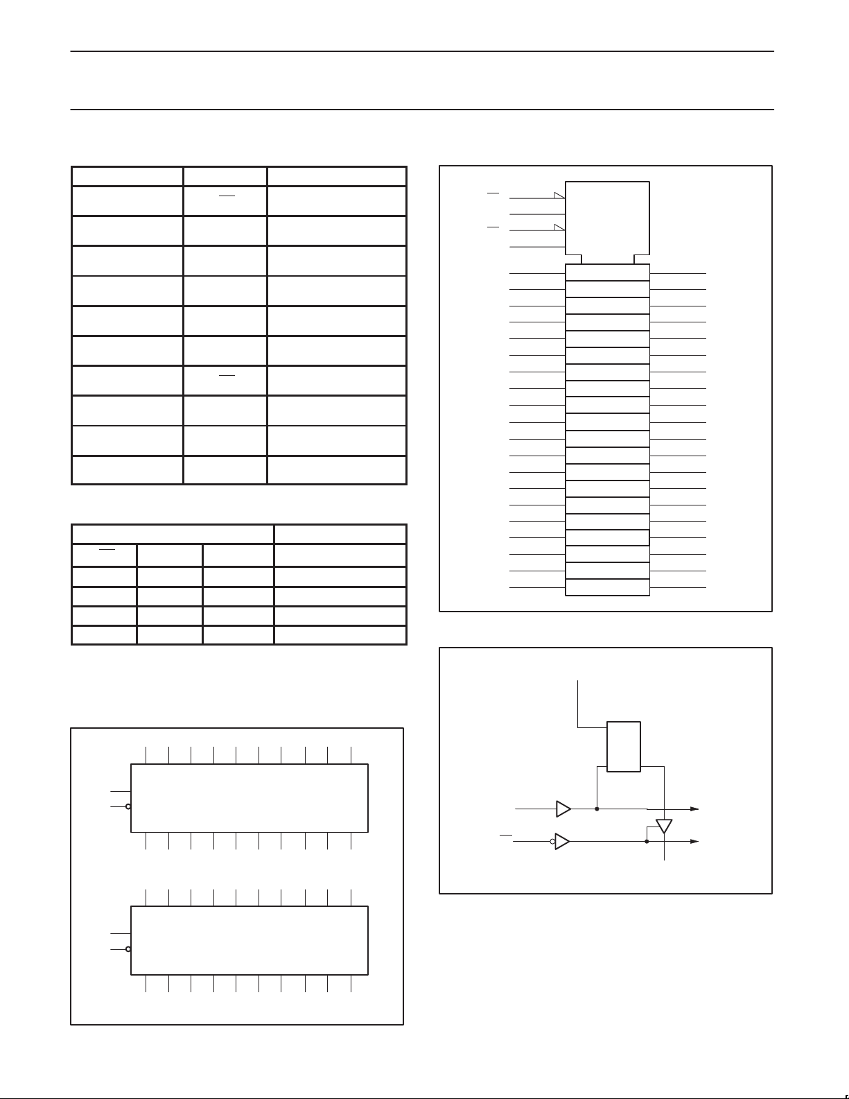
LOGIC SYMBOL (IEEE/IEC)
1
1OE
56
1LE
28
2OE
29
2LE
55
1D0
54
1D1
52
1D2
51
1D3
49
1D4
48
1D5
47
1D6
45
1D7
44
1D8
43
1D9
42
2D0
41
2D1
40
2D2
38
2D3
37
2D4
36
2D5
34
2D6
33
2D7
31
2D8
30
2D9
0
1D
3D
EN2
C1
EN4
C3
2 ∇
4 ∇
2
1Q0
3
1Q1
5
1Q2
6
1Q3
8
1Q4
9
1Q5
10
1Q6
12
1Q7
13
1Q8
14
1Q9
15
2Q0
16
2Q1
17
2Q2
19
2Q3
20
2Q4
21
2Q5
23
2Q6
24
2Q7
26
2Q8
27
2Q9
SH00152
LOGIC DIAGRAM
nD
0
LOGIC SYMBOL
55 54 52 51 49 48 47 45 44 43
1D0 1D1 1D2 1D3 1D4 1D5 1D6 1D7
1LE
56
1OE
1
1Q0 1Q1 1Q2 1Q3 1Q4 1Q5 1Q6 1Q7
2 3 5 6 8 9 10 12 13 14
42 41 40 38 37 36 34 33 31 30
2D0 2D1 2D2 2D3 2D4 2D5 2D6 2D7
2LE
29
2OE
28
2Q0 2Q1 2Q2 2Q3 2Q4 2Q5 2Q6 2Q7
15 16 17 19 20 21 23 24 26 27
1998 Jul 27
1D8 1D9
1Q8 1Q9
2D8 2D9
2Q8 2Q9
SH00023
D
LE
nLE
nOE
nQ
0
SH00151
3
 Loading...