

Philips 74ALVCH16827DL, 74ALVCH16827DGG Datasheet
74ALVCH16827
20-bit buffer/line driver, non-inverting
(3-State)
Product specification
IC24 Data Handbook
1998 Jul 27
INTEGRATED CIRCUITS
Philips Semiconductors Product specification
74ALVCH1682720-bit buffer/line driver, non-inverting (3-State)
2
1998 Jul 27 853-2096 19785
FEA TURES
•Wide supply voltage range of 1.2V to 3.6V
•Complies with JEDEC standard no. 8-1A
•Wide supply voltage range of 1.2V to 3.6V
•CMOS low power consumption
•Direct interface with TTL levels
•Universal bus transceiver with D-type latches and D-type flip-flops
capable of operating in transparent, latched, clocked or
clocked-enabled mode.
•MULTIBYTE
TM
flow-through standard pin-out architecture
•Low inductance multiple V
CC
and GND pins for minimum noise
and ground bounce
•Current drive ±24 mA at 3.0 V
•All inputs have bus hold circuitry
•Output drive capability 50Ω transmission lines @ 85°C
•3-State non-inverting outputs for bus oriented applications
DESCRIPTION
The 74ALVCH16827 is a 20-bit non-inverting buf fer/driver with
3-State outputs for bus oriented applications.
The 74ALVCH16827 consists of two 10-bit sections with separate
output enable signals. For either 10-bit buffer section, the two output
enable (1OE
1 and 1OE2 or 2OE1 and 2OE2) inputs must both be
active. If either output enable input is high, the outputs of that 10-bit
buffer section are in high impedance state.
The 74ALVCH16827 has active bus hold circuitry which is provided
to hold unused or floating data inputs at a valid logic level. This
feature eliminates the need for external pull-up or pull-down
resistors.
QUICK REFERENCE DA TA
GND = 0V; T
amb
= 25°C; tr = tf = 2.5ns
SYMBOL
PARAMETER CONDITIONS TYPICAL UNIT
t
PHL/tPLH
Propagation delay
CP to Qn
VCC = 2.5V , CL = 30pF
V
CC
= 3.3V , CL = 50pF
2.0
2.0
ns
C
I
Input capacitance 5 pF
p
p
p
1
Output enabled 20
p
CPDPower dissi ation ca acitance er latch
V
I
=
GND to V
CC
1
Output disabled 3
F
NOTES:
1. C
PD
is used to determine the dynamic power dissipation (PD in W):
P
D
= CPD × V
CC
2
× fi + (CL × V
CC
2
× fo) where:
f
i
= input frequency in MHz; CL = output load capacity in pF;
f
o
= output frequency in MHz; VCC = supply voltage in V;
(C
L
× V
CC
2
× fo) = sum of outputs.
ORDERING INFORMATION
PACKAGES TEMPERATURE RANGE OUTSIDE NORTH AMERICA NORTH AMERICA DWG NUMBER
56-Pin Plastic TSSOP Type II –40°C to +85°C 74ALVCH16827 DGG ACH16827 DGG SOT364-1
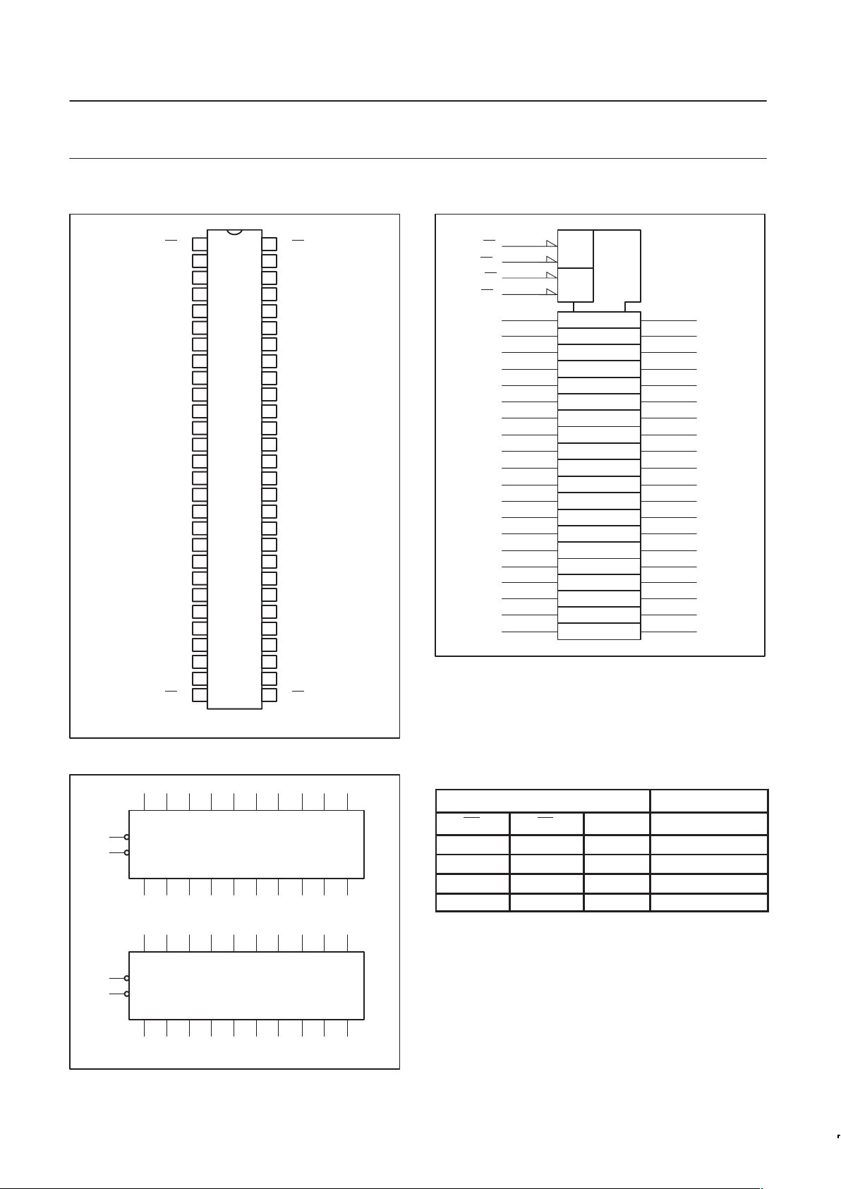
PIN DESCRIPTION
PIN NUMBER SYMBOL FUNCTION
55, 54, 52, 51, 49, 48, 47, 45, 44, 43,
42, 41, 40, 38, 37, 36, 34, 33, 31, 30
1A0 - 1A9
2A0 - 2A9
Data inputs
2, 3, 5, 6, 8, 9, 10, 12, 13, 14,
15, 16, 17, 19, 20, 21, 23, 24, 26, 27
1Y0 - 1Y9
2Y0 - 2Y9
Data outputs
1, 56,
28, 29
1OE0, 1OE1
2OE0, 2OE1
Output enable inputs (active-Low)
4, 11, 18, 25, 32, 39, 46, 53 GND Ground (0V)
7, 22, 35, 50 V
CC
Positive supply voltage
Philips Semiconductors Product specification
74ALVCH16827
20-bit buffer/line driver, non-inverting (3-State)
1998 Jul 27
3
PIN CONFIGURATION
1
2
3
4
5
6
7
8
9
10
11
12
13
14
15
16
17
18
19
20
21
22
23
24
25
26
27
28 29
30
31
32
33
34
35
36
37
38
39
40
41
42
43
44
45
46
47
48
49
50
51
52
53
54
55
561OE1
1Y0
1Y1
1Y2
1Y3
1Y4
1Y5
1Y6
GND
V
CC
GND
1Y7
1Y8
1Y9
2Y0
2Y1
2Y2
GND
2Y3
2Y4
2Y5
V
CC
2Y6
2Y7
GND
2Y8
2Y9
2OE
1
1OE
2
1A0
1A1
GND
1A2
1A3
V
CC
1A4
1A5
1A6
GND
1A7
1A8
1A9
2A0
2A1
2A2
GND
2A3
2A4
2A5
V
CC
2A6
2A7
GND
2A8
2A9
2OE
2
SH00010
LOGIC SYMBOL
1A0 1A1 1A2 1A3 1A4 1A5 1A6 1A7
1Y0 1Y1 1Y2 1Y3 1Y4 1Y5 1Y6 1Y7
1A8 1A9
1Y8 1Y9
2A0 2A1 2A2 2A3 2A4 2A5 2A6 2A7
2Y0 2Y1 2Y2 2Y3 2Y4 2Y5 2Y6 2Y7
2A8 2A9
2Y8 2Y9
55 54 52 51 49 48 47 45 44 43
56
1
29
28
2 3 5 6 8 9 10 12 13 14
42 41 40 38 37 36 34 33 31 30
15 16 17 19 20 21 23 24 26 27
SH00011
1OE1
1OE2
2OE1
2OE2
LOGIC SYMBOL (IEEE/IEC)
EN1
1 ∇
EN2
1
2 ∇
1
SH00012
1
56
28
29
55
54
52
51
49
48
47
45
44
43
42
41
40
38
37
36
34
33
31
30
2
3
5
6
8
9
10
12
13
14
15
16
17
19
20
21
23
24
26
27
&
&
1OE1
1Y0
1Y1
1Y2
1Y3
1Y4
1Y5
1Y6
1Y7
1Y8
1Y9
2Y0
2Y1
2Y2
2Y3
2Y4
2Y5
2Y6
2Y7
2Y8
2Y9
2OE
1
1OE
2
1A0
1A1
1A2
1A3
1A4
1A5
1A6
1A7
1A8
1A9
2A0
2A1
2A2
2A3
2A4
2A5
2A6
2A7
2A8
2A9
2OE
2
FUNCTION TABLE
INPUTS OUTPUTS
nOE1 nOE2 A Y
L L L L
L L H H
H H X Z
X H X Z
H = High voltage level
L = Low voltage level
X = Don’t care
Z = High impedance “off” state
 Loading...