

Philips 74alvch16823 DATASHEETS

INTEGRATED CIRCUITS
74ALVCH16823
18-bit bus-interface D-type flip-flop
with reset and enable (3-State)
Product specification
IC24 Data Handbook
1998 Jul 29
Philips Semiconductors Product specification
CPDPower dissipation capacitance per latch
V
GND to V
1
pF
18-bit D-type flip-flop (3-State)
FEA TURES
•Wide supply voltage range of 1.2V to 3.6V
•Complies with JEDEC standard no. 8-1A.
•CMOS low power consumption
•Direct interface with TTL levels
•Current drive ± 24 mA at 3.0 V
•Multibyteflow-through standard pin-out architecture
•Low inductance multiple V
ground bounce
•All data inputs have bus hold
•Output drive capability 50Ω transmission lines @ 85°C
and GND pins to minimize noise and
CC
74AL VCH16823
DESCRIPTION
The 74ALVCH16823 is a 18-bit edge-triggered flip-flop featuring
separate D-type inputs for each flip-flop and 3-state outputs for bus
oriented applications. Incorporates bushold data inputs which
eliminate the need for external pull-up resistors to hold unused
inputs. The74ALVCH16823 consists of two sections of nine
edge-triggered flip-flops. A clock (CP) input, an output-enable (OE
input, a Master reset (MR
provided for each total 9-bit section.
With the clock-enable (CE
the state of their individual D-inputs that meet the set-up and hold
time requirements on the LOW-to-HIGH CP transition. Taking CE
HIGH disables the clock buffer, thus latching the outputs. Taking the
Master reset (MR
independently of the clock.
When OE
outputs. When the OE
impedance OFF-state. Operation of the OE
state of flip-flops.
Active bus hold circuitry is provided to hold unused or floating data
inputs at a valid logic level.
is LOW, the contents of the flip-flops are available at the
) input and a clock-enable( CE) input are
) input LOW, the D-type flip-flops will store
) input LOW causes all the Q outputs to go LOW
is HIGH, the outputs go to the high
input does not affect the
)
QUICK REFERENCE DATA
GND = 0V; T
SYMBOL
t
PHL/tPLH
F
max
C
I
NOTES:
1. C
PD
P
D
f
= input frequency in MHz; CL = output load capacity in pF;
i
= output frequency in MHz; VCC = supply voltage in V;
f
o
(C
= 25°C; tr = tf ≤ 2.5ns
amb
PARAMETER CONDITIONS TYPICAL UNIT
Propagation delay
CP to Qn
Maximum clock frequency
Input capacitance 5.0 pF
p
is used to determine the dynamic power dissipation (PD in W):
= CPD × V
× V
L
2
× fi + (CL × V
CC
2
× fo) = sum of outputs.
CC
p
2
× fo) where:
CC
p
VCC = 2.5V, CL = 30pF
VCC = 3.3V, CL = 50pF
VCC = 2.5V, CL = 30pF
VCC = 3.3V, CL = 50pF
=
I
CC
2.1
2.1
300
350
Outputs enabled 16
Outputs disabled 10
ORDERING INFORMATION
PACKAGES TEMPERATURE RANGE OUTSIDE NORTH AMERICA NORTH AMERICA DWG NUMBER
56-Pin Plastic SSOP Type II -40°C to +85°C 74ALVCH16823 DL ACH16823 DL SOT371-1
56-Pin Plastic TSSOP Type II -40°C to +85°C 74ALVCH16823 DGG ACH16823 DGG SOT364-1
ns
MHz
p
1998 Jul 29 853–2100 19800
2
Philips Semiconductors Product specification
18-bit D-type flip-flop (3-State)
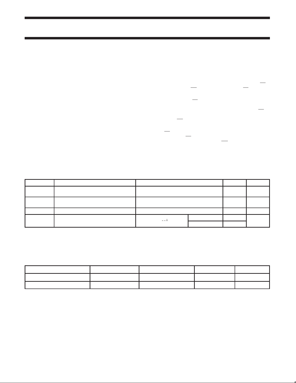
PIN DESCRIPTION
PIN NUMBER SYMBOL FUNCTION
2, 27 1OE, 2OE Output enable input (active-Low)
54, 52, 51, 49, 48, 47, 45, 44, 43
42, 41, 40, 38, 37, 36, 34, 33, 31
3, 5, 6, 8, 9, 10, 12, 13, 14
15, 16, 17, 19, 20, 21, 23, 24, 26
56, 29 1CP, 2CP Clock pulse input (active rising edge)
55, 30 1CE, 2CE Clock enable input (active-Low)
1, 28 1MR, 2MR Master reset input (active-Low)
4, 11, 18, 25, 32, 39, 46, 53 GND Ground (0V)
7, 22, 35, 50 V
PIN CONFIGURATION
1
2
1OE
3
1Q0
GND
4
5
1Q1
6
1Q2
V
7
CC
8
1Q3
9
1Q4
10
1Q5
11
GND
12
1Q6
13
1Q7
14
1Q8
15
2Q0
16
2Q1
17
2Q2
18
GND
19
2Q3
20
2Q4
21
2Q5
22
V
CC
23
2Q6
24
2Q7
25
GND
26
2Q8
27
2OE
28 29
2MR
561MR
1CP
55
1CE
54
1D0
53
GND
52
1D1
51
1D2
50
V
CC
49
1D3
48
1D4
47
1D5
46
GND
45
1D6
44
1D7
43
1D8
42
2D0
41
2D1
40
2D2
39
GND
38
2D3
37
2D4
36
2D5
35
V
CC
34
2D6
33
2D7
32
GND
31
2D8
30
2CE
2CP
1D0-1D8
2D0-2D8
1Q0-1Q8
2Q0-2Q8
CC
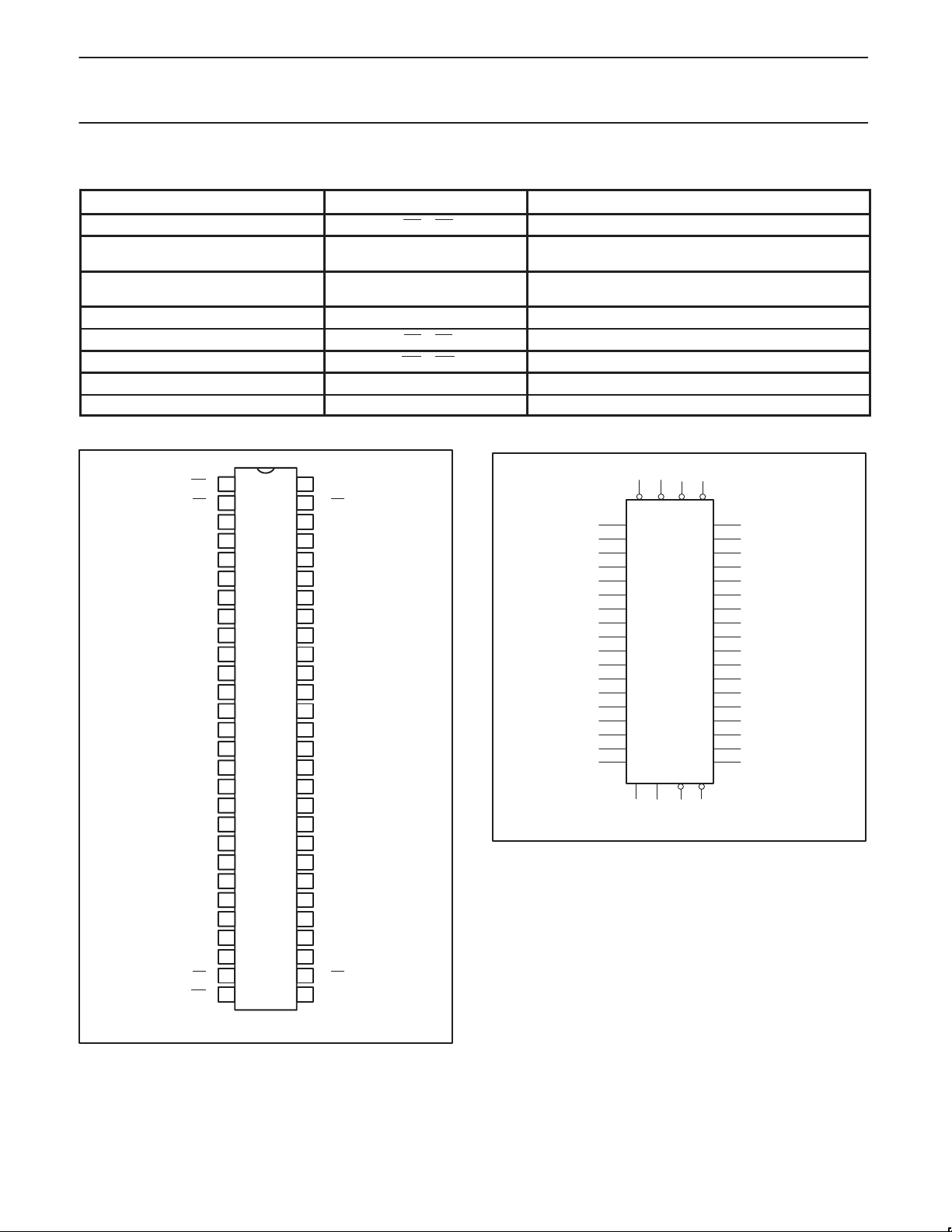
LOGIC SYMBOL
Data inputs
Data outputs
Positive supply voltage
128227
1MR2MR 1OE 2OE
54
52
51
49
48
47
45
44
43
42
41
40
38
37
36
34
33
31
A0
A1
A2
A3
A4
A5
A6
A7
A8
A9
A10
A11
A12
A13
A14
A15
A16
A17
1CP 2CP 1CE 2CE
48 29 55 30
74ALVCH16823
B0
B1
B2
B3
B4
B5
B6
B7
B8
B9
B10
B11
B12
B13
B14
B15
B16
B17
3
5
6
8
9
10
12
13
14
15
16
17
19
20
21
23
24
26
SW00341
1998 Jul 29
SH00014
3
Philips Semiconductors Product specification
18-bit D-type flip-flop (3-State)
LOGIC SYMBOL (IEEE/IEC)
1OE
1MR
1CE
1CP
2OE
2MR
2CE
2CP
1D0
1D1
1D2
1D3
1D4
1D5
1D6
1D7
1D8
2D0
2D1
2D2
2D3
2D4
2D5
2D6
2D7
2D8
2
1
55
56
27
28
30
29
54
52
51
49
48
47
45
44
43
42
41
40
38
37
36
34
33
31
EN1
R2
G3
EN5
R6
G7
4D
8D
3C4
7C8
1, 2 ∇
5, 6 ∇
3
5
6
8
9
10
12
13
14
15
16
17
19
20
21
23
24
25
SH00015
1Q0
1Q1
1Q2
1Q3
1Q4
1Q5
1Q6
1Q7
1Q8
2Q0
2Q1
2Q2
2Q3
2Q4
2Q5
2Q6
2Q7
2Q8
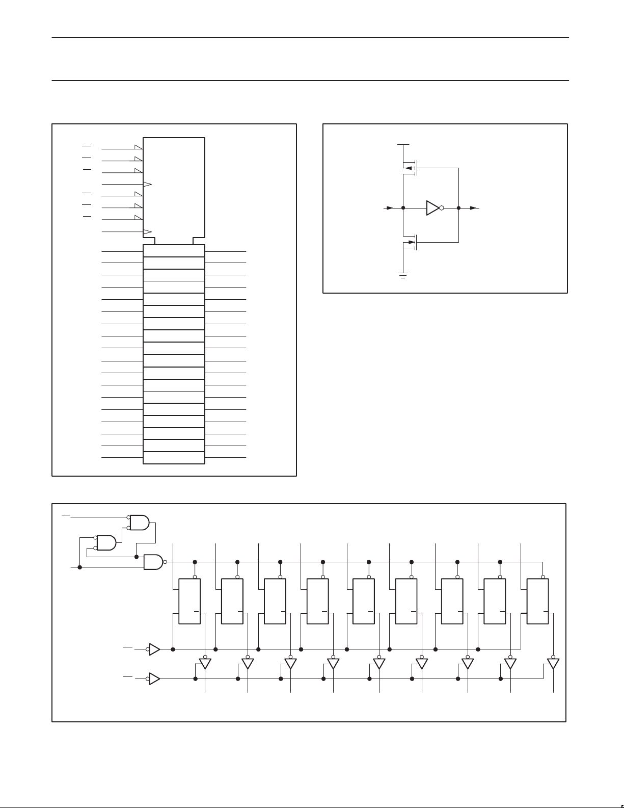
BUS HOLD CIRCUIT
V
CC
Data Input
74ALVCH16823
To internal circuit
SW00044
LOGIC DIAGRAM
nCE
nCP
nMR
nOE
n = 1 or 2
1998 Jul 29
nD0
nD1
CP CP CP CP CP CP CP CP CP
nD
R
nD
R
Q
nQ0
nD2
Q Q Q Q Q Q Q Q
nQ1
nD3
nD
R
nD
R
nQ2
nQ3
nD4
nD5
nD
R
nD
R
nQ4
nQ5
nD6
nD7
nD
R
nD
R
nQ6
4
nQ7
nD8
nD
R
nQ8
SH00016
 Loading...