

Philips 74ALVCH16821DGG, 74ALVCH16821DL Datasheet

INTEGRATED CIRCUITS
74ALVCH16821
20-bit bus-interface D-type flip-flop;
positive-edge trigger (3-State)
Product specification
IC24 Data Handbook
1998 May 29
Philips Semiconductors Product specification
CPDPower dissipation capacitance per buffer
V
GND to V
1
pF
20-bit bus-interface D-type flip-flop;
positive-edge trigger (3-State)
FEA TURES
•Wide supply voltage range of 1.2V to 3.6V
•Complies with JEDEC standard no. 8-1A
•Current drive ± 24 mA at 3.0 V
•CMOS low power consumption
•Direct interface with TTL levels
•MULTIBYTE
•Low inductance multiple V
and ground bounce
•All data inputs have bus hold
•Output drive capability 50Ω transmission lines @ 85°C
QUICK REFERENCE DATA
GND = 0V; T
SYMBOL
t
PHL/tPLH
C
I
F
max
NOTE:
1. C
P
f
= input frequency in MHz; CL = output load capacitance in pF;
i
f
o
(C
TM
flow-through standard pin-out architecture
and ground pins for minimum noise
CC
= 25°C; tr = tf ≤ 2.5ns
amb
PARAMETER CONDITIONS TYPICAL UNIT
Propagation delay
nCP to nQ
Input capacitance 5.0 pF
Maximum clock frequency
is used to determine the dynamic power dissipation (PD in W):
PD
= CPD × V
D
= output frequency in MHz; VCC = supply voltage in V;
L
CC
2
× V
× fo) = sum of outputs.
CC
n
p
2
× fi + (CL × V
p
2
× fo) where:
CC
p
DESCRIPTION
The 74ALVCH16821 has two 10-bit, edge triggered registers, with
each register coupled to a 3-State output buffer. The two sections of
each register are controlled independently by the clock (nCP) and
Output Enable (nOE
Each register is fully edge triggered. The state of each D input, one
set-up time before the Low-to-High clock transition, is transferred to
the corresponding flip-flop’s Q output.
When nOE
When nOE
Operation of the nOE
The 74ALVCH16821 has active bus hold circuitry which is provided
to hold unused or floating data inputs at a valid logic level. This
feature eliminates the need for external pull-up or pull-down
resistors.
VCC = 2.5V, CL = 30pF
VCC = 3.3V, CL = 50pF
=
I
VCC = 2.5V, CL = 30pF
VCC = 3.3V, CL = 50pF
CC
74AL VCH16821
) control gates.
is LOW, the data in the register appears at the outputs.
is HIGH, the outputs are in high impedance OFF state.
input does not affect the state of the flip-flops.
2.6
2.5
Outputs enabled 33
Outputs disabled 17
250
350
ns
p
MHz
ORDERING INFORMATION
PACKAGES TEMPERATURE RANGE OUTSIDE NORTH AMERICA NORTH AMERICA DWG NUMBER
56-Pin Plastic SSOP Type III –40°C to +85°C 74ALVCH16821 DL ACH16821 DL SOT371-1
56-Pin Plastic TSSOP Type II –40°C to +85°C 74ALVCH16821 DGG ACH16821 DGG SOT364-1
1998 May 29 853-2066 19467
2
Philips Semiconductors Product specification
Data in uts
Data out uts
20-bit bus-interface D-type flip-flop;
positive-edge trigger (3-State)
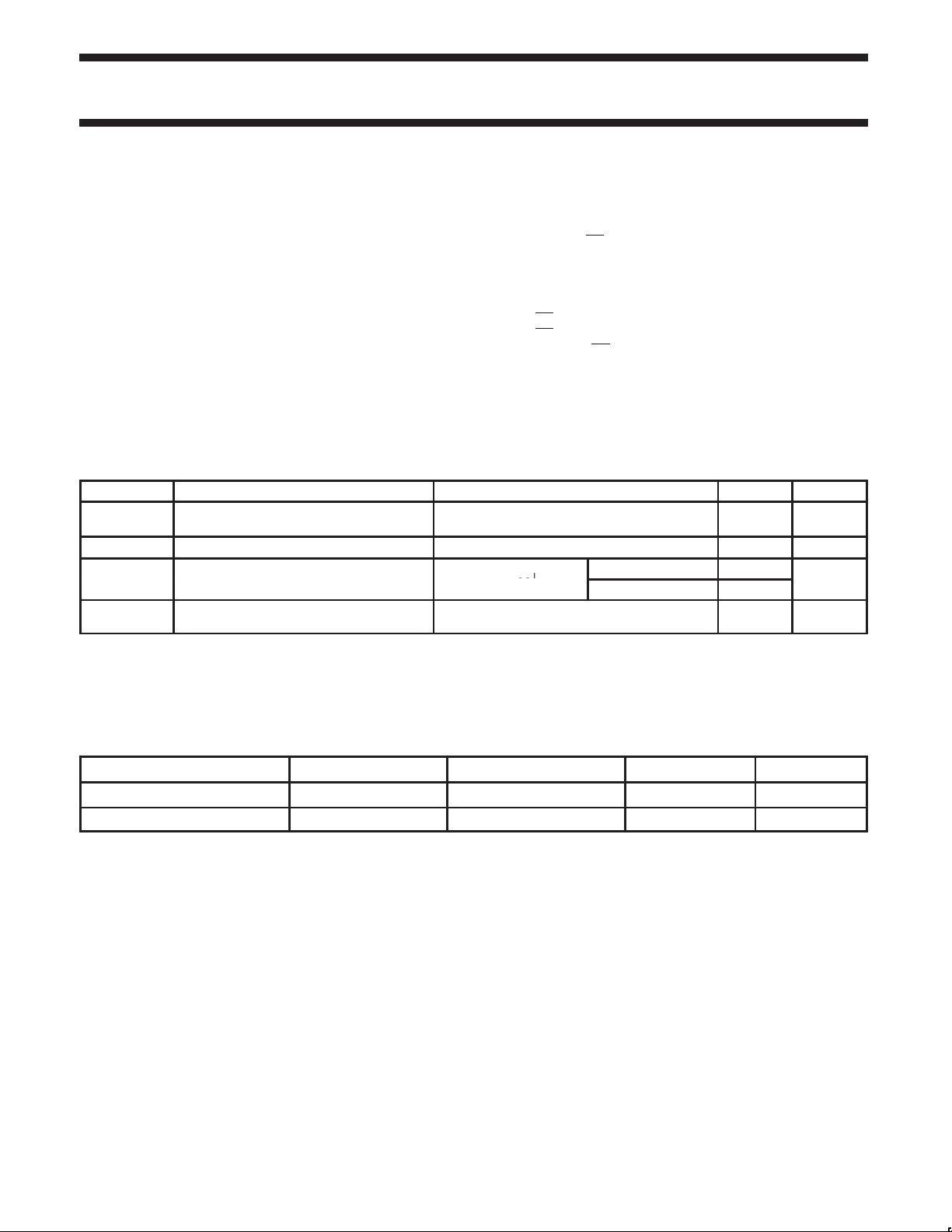
PIN DESCRIPTION
PIN NUMBER SYMBOL FUNCTION
55, 54, 52, 51, 49,
48, 47, 45, 44, 43
42, 41, 40, 38, 37,
36, 34, 33, 31, 30
2, 3, 5, 6, 8,
9, 10, 12, 13, 14
15, 16, 17, 19, 20,
21, 23, 24, 26, 27
1, 28 1OE, 2OE
56, 29 1CP, 2CP
4, 11, 18, 25,
32, 39, 46, 53
7, 22, 35, 50 V
PIN CONFIGURATION
1D0 - 1D9
2D0 - 2D9
1Q0 - 1Q9
2Q0 - 2Q9
1
1Q0
2
1Q1
3
GND
4
1Q2
5
1Q3
6
V
7
CC
1Q4
8
1Q5
9
1Q6
10
GND
11
1Q7
12
1Q8
13
1Q9
14
2Q0
15
2Q1
16
2Q2
17
GND
18
2Q3
19
2Q4
20
2Q5
21
V
22
CC
23
2Q6
24
2Q7
25
GND
26
2Q8
27
2Q9
28 29
2OE
p
p
Output enable inputs
(active-Low)
Clock pulse inputs
(active rising edge)
GND Ground (0V)
CC
Positive supply
voltage
561OE
1CP
55
1D0
54
1D1
53
GND
52
1D2
51
1D3
50
V
CC
1D4
49
1D5
48
1D6
47
GND
46
1D7
45
1D8
44
1D9
43
2D0
42
2D1
41
2D2
40
GND
39
2D3
38
2D4
37
2D5
36
V
35
CC
34
2D6
33
2D7
32
GND
31
2D8
30
2D9
2CP
74ALVCH16821
FUNCTION TABLE
INPUTS OUTPUT
nOE CP Dx Q
L ↑ L L
L ↑ H H
L
H X X Z
H = HIGH voltage level
L = LOW voltage level
X = Don’t care
Z = High impedance OFF state
↑ = LOW to HIGH clock transition
= Not a LOW-to-HIGH clock transition
LOGIC SYMBOL
2
1Q0
1Q1
3
1Q2
5
6
1Q3
1Q4
8
1Q5
9
1Q6
10
1Q7
12
13
1Q8
14
1Q9
2Q0
15
2Q1
16
2Q2
17
2Q3
19
20
2Q4
21
2Q5
2Q6
23
24
2Q7
2Q8
26
2Q9
27
X Q0
1
2OE
56
1CP1OE
2CP
2928
1D0
1D1
1D2
1D3
1D4
1D5
1D6
1D7
1D8
1D9
2D0
2D1
2D2
2D3
2D4
2D5
2D6
2D7
2D8
2D9
55
54
52
51
49
48
47
45
44
43
42
41
40
38
37
36
34
33
31
30
SH00127
1998 May 29
SH00001
3
Philips Semiconductors Product specification
20-bit bus-interface D-type flip-flop;
positive-edge trigger (3-State)
LOGIC SYMBOL (IEEE/IEC)
1OE
1CP
2OE
2CP
1D0
1D1
1D2
1D3
1D4
1D5
1D6
1D7
1D8
1D9
2D0
2D1
2D2
2D3
2D4
2D5
2D6
2D7
2D8
2D9
1
56
28
29
55
54
52
51
49
48
47
45
44
43
42
41
40
38
37
36
34
33
31
30
EN2
EN4
1D
3D
C1
C3
2 ∇
4 ∇
2
3
5
6
8
9
10
12
13
14
15
16
17
19
20
21
23
24
26
27
SH00003
1Q0
1Q1
1Q2
1Q3
1Q4
1Q5
1Q6
1Q7
1Q8
1Q9
2Q0
2Q1
2Q2
2Q3
2Q4
2Q5
2Q6
2Q7
2Q8
2Q9
74ALVCH16821
LOGIC DIAGRAM
nD0
D
CP Q
nCP
nOE
nQ0
nD1
D
CP Q
nQ1
nD2
D
CP Q
nQ2
nD3
D
CPQ
nQ3
nD4
D
CP Q
nQ4
nD5
D
CPQ
nQ5
nD6
D
CP Q
nQ6
nD7
D
CPQ
nQ7
nD8
D
CPQ
nQ8
nD9
D
CPQ
nQ9
SH00004
1998 May 29
4
 Loading...