

Philips 74ALVCH16543DGG Datasheet

INTEGRATED CIRCUITS
DATA SH EET
74ALVCH16543
16-bit D-type registered
transceiver; 3-state
Product specification
Supersedes data of 1998 Aug 31
File under Integrated Circuits, IC24
1999 Nov 23
Philips Semiconductors Product specification
16-bit D-type registered transceiver; 3-state 74ALVCH16543
FEATURES
• In accordance with JEDEC standard no 8-1A
• CMOS low power consumption
• Direct interface with TTL levels
• MULTIBYTE flow-through pin-out architecture
• 16-bit transceiver with D-type latch
• Combines 16245 and 16373 type functions in one chip
• Back-to-back registers for storage
• Output drive capability 50 Ω transmission lines at 85 °C
• Separate controls for data flow in each direction
• All data inputs have bus hold
• 3-state non-inverting outputs for bus oriented
applications
• Current drive ±24 mA at 3.0 V.
DESCRIPTION
The74ALVCH16543isadualoctalregisteredtransceiver.
Each section contains two sets of D-type latches for
temporary storage of the data flow in either direction.
Separate latch enable (nLEAB, nLEBA) and output enable
(nOEAB, nOEBA) inputs are provided for each register to
permit independent control in either direction of the data
flow.
The ‘16543’ contains two sections each consisting of two
sets of eight D-type latches with separate inputs and
controls for each set. For data flow from A to B, for
example, the A-to-Benable (nEAB, where nequals 1 or 2)
inputsmust beLOW inorder toenterdata fromnA0to nA7,
or take data from nB0to nB7, as indicated in the function
table. With nEAB LOW, a LOW signal on the A-to-B latch
enable (nLEAB) input makes the A-to-B latches
transparent; a subsequent LOW-to-HIGH transition of the
nLEABsignal storestheA data into the latches.With nE
AB
and nOEAB both LOW, the 3-state B output buffers are
active and display the data present at the output of the
A latches. Similarly, the nEBA, nLEBA and nOEBA signals
control the data flow from B-to-A.
Active bus hold circuitry is provided to hold unused or
floating data inputs at a valid logic level.
FUNCTION TABLE
See note 1.
INPUTS
OUTPUTS STATUS
n
OE
XX
nE
XX
nLE
XX
nBn,nA
n
H X X X Z disabled
X H X X Z disabled
L ↑ L h Z disabled and latch
L ↑ Ll Z
LL↑h H latch and display
LL↑lL
L L L H H transparent
LLLL L
L L H X NC hold
Note
1. XX = AB for A-to-B direction, BA for B-to-A direction;
H = HIGH voltage level; L = LOW voltage level;
h = HIGH state mustbepresent one set-up time beforetheLOW-to-HIGH transition of nLEAB,nLEBA,nEABor nEBA;
l = LOW state must be present one set-up time before the LOW-to-HIGH transition of nLEAB, nLEBA, nEAB or nEBA;
X = don’t care; NC = no change;
↑ = LOW-to-HIGH level transition;
Z = high-impedance OFF-state.
1999 Nov 23 2
Philips Semiconductors Product specification
16-bit D-type registered transceiver; 3-state 74ALVCH16543
QUICK REFERENCE DATA
Ground = 0; T
SYMBOL PARAMETER CONDITIONS TYPICAL UNIT
t
PHL/tPLH
C
I
C
PD
Notes
1. C
is used to determine the dynamic power dissipation (PDin µW).
PD
PD=CPD× V
= input frequency in MHz;
f
i
CL= output load capacitance in pF;
fo= output frequency in MHz;
VCC= supply voltage in Volts;
Σ (CL× V
2. The condition is VI= GND to VCC.
=25°C; tr=tf= 2.5 ns
amb
propagation delay nAn,nBnto nBn,nA
n
CL= 50 pF;
3.8 ns
VCC= 3.3 V
input capacitance 4.0 pF
power dissipation capacitance per latch notes 1 and 2
outputs enabled 44 pF
outputs disabled 14 pF
2
× fi+ Σ (CL× V
CC
2
× fo) = sum of outputs.
CC
2
× fo) where:
CC
ORDERING INFORMATION
PACKAGE
OUTSIDE NORTH
AMERICA
NORTH
AMERICA
TEMPERATURE
RANGE
PINS PACKAGE MATERIAL CODE
74ALVCH16543DGG ACH16543 DGG −40 to +85 °C 56 TSSOP plastic SOT364-1
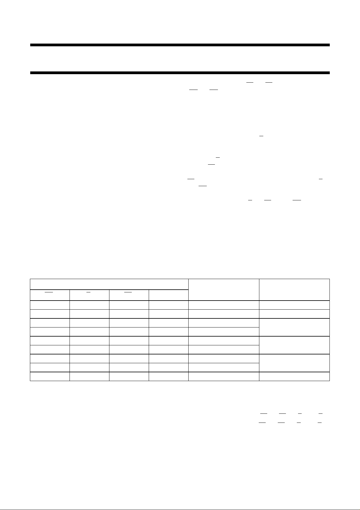
PINNING
PIN SYMBOL DESCRIPTION
1 and 28 1
2 and 27 1
3 and 26 1
OEAB, 2OE
LEAB, 2LE
EAB, 2E
AB
AB
AB
output enable A-to-B for register 1 or 2
latch enable A-to-B for register 1 or 2
A-to-B enable for register 1 or 2
4, 11, 18, 25, 32, 39, 46 and 53 GND ground (0 V)
5, 6, 8, 9, 10, 12, 13 and 14 1A
7, 22, 35 and 50 V
15, 16, 17, 19, 20, 21, 23 and 24 2A
29 and 56 2
30 and 55 2
31 and 54 2
33, 34, 36, 37, 38, 40, 41 and 42 2B
43, 44, 45, 47, 48, 49, 51 and 52 1B
to 1A
0
7
CC
to 2A
0
7
OEBA, 1OE
LEBA, 1LE
EBA, 1E
to 2B
7
to 1B
7
BA
0
0
AB
BA
data inputs/outputs
DC supply voltage
data inputs/outputs
output enable B-to-A for register 1 or 2
latch enable B-to-A for register 1 or 2
B-to-A enable for register 1 or 2
data inputs/outputs
data inputs/outputs
1999 Nov 23 3
Philips Semiconductors Product specification
16-bit D-type registered transceiver; 3-state 74ALVCH16543
handbook, halfpage
1OE
1LE
1E
2E
2LE
2OE
AB
AB
AB
GND
1A
1A
V
CC
1A
1A
1A
GND
1A
1A
1A
2A
2A
2A
GND
2A
2A
2A
V
CC
2A
2A
GND
AB
AB
AB
1OE
MNA297
56
BA
1LE
55
BA
1E
54
BA
GND
53
1B
52
0
1B
51
1
V
50
CC
1B
49
2
1B
48
3
1B
47
4
GND
46
1B
45
5
1B
44
6
1B
43
7
2B
42
0
2B
41
1
2B
40
2
GND
39
2B
38
3
2B
37
4
2B
36
5
V
35
CC
2B
34
6
2B
33
7
GND
32
2E
31
BA
2LE
30
BA
2OE
29
BA
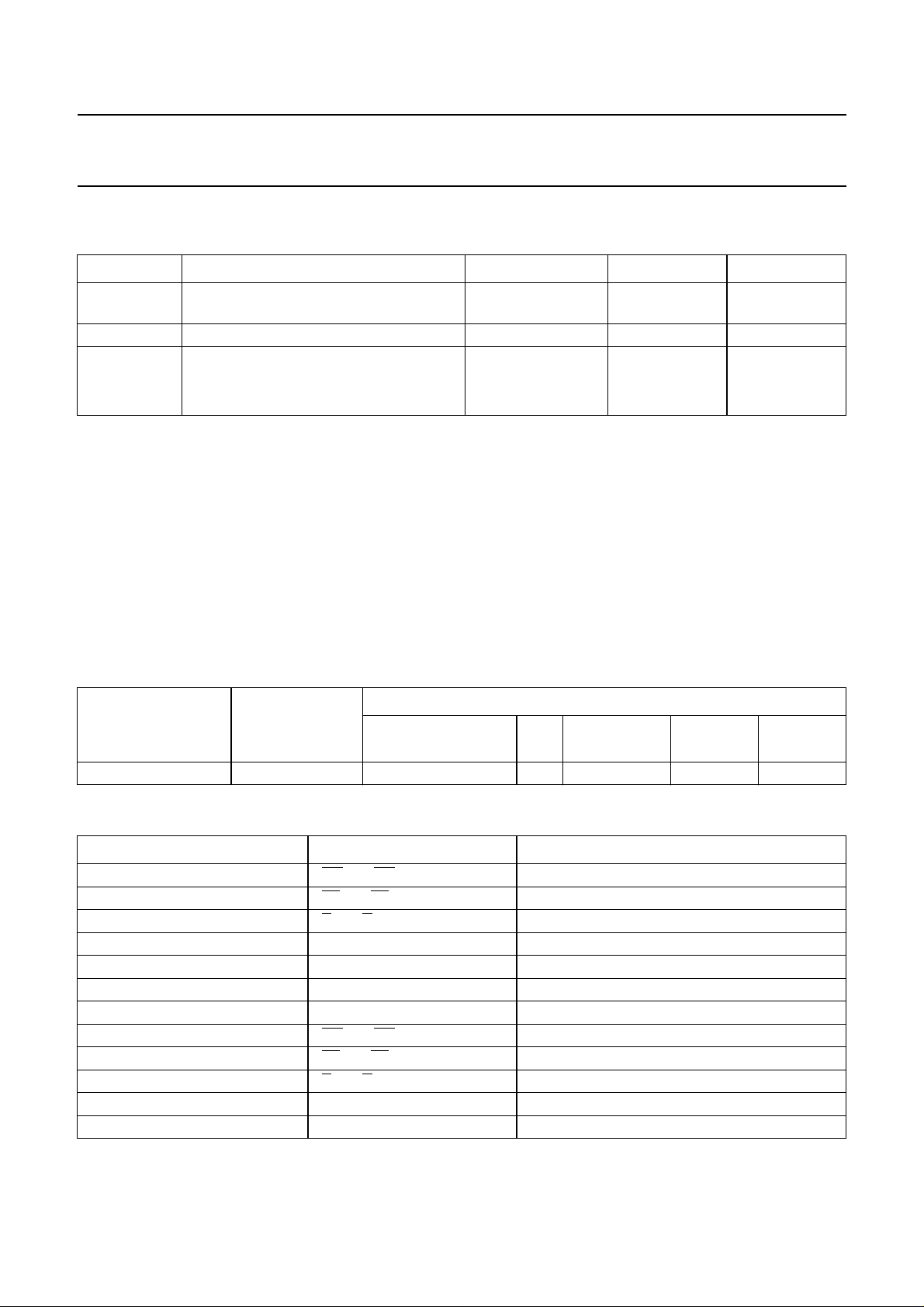
handbook, halfpage
data
input
V
CC
MNA300
Fig.2 Bus hold circuit.
to internal circuit
1
2
3
4
5
0
6
1
7
8
2
9
3
10
4
11
12
5
13
6
14
7
0
1
2
3
4
5
6
7
16543
15
16
17
18
19
20
21
22
23
24
25
26
27
28
Fig.1 Pin configuration.
1999 Nov 23 4
Philips Semiconductors Product specification
16-bit D-type registered transceiver; 3-state 74ALVCH16543
handbook, full pagewidth
1A
0
5
1A
1
6
1A
2
8
1A
3
9
1A
4
10
1A
5
12
1A
6
13
1A
7
14
1OE
56
54
55
BA
1OE
AB
1
1E
AB
3
1E
BA
1LE
AB
2
1LE
BA
1B
1B
1B
1B
1B
1B
1B
1B
0
52
1
51
2
49
3
48
4
47
5
45
6
44
7
43
2A
0
15
2A
1
16
2A
2
17
2A
3
19
2A
4
20
2A
5
21
2A
6
23
2A
7
24
2OE
BA
29
2OE
AB
28
2E
AB
26
2E
BA
31
2LE
AB
27
2LE
BA
30
2B
2B
2B
2B
2B
2B
2B
2B
MNA298
0
42
1
41
2
40
3
38
4
37
5
36
6
34
7
33
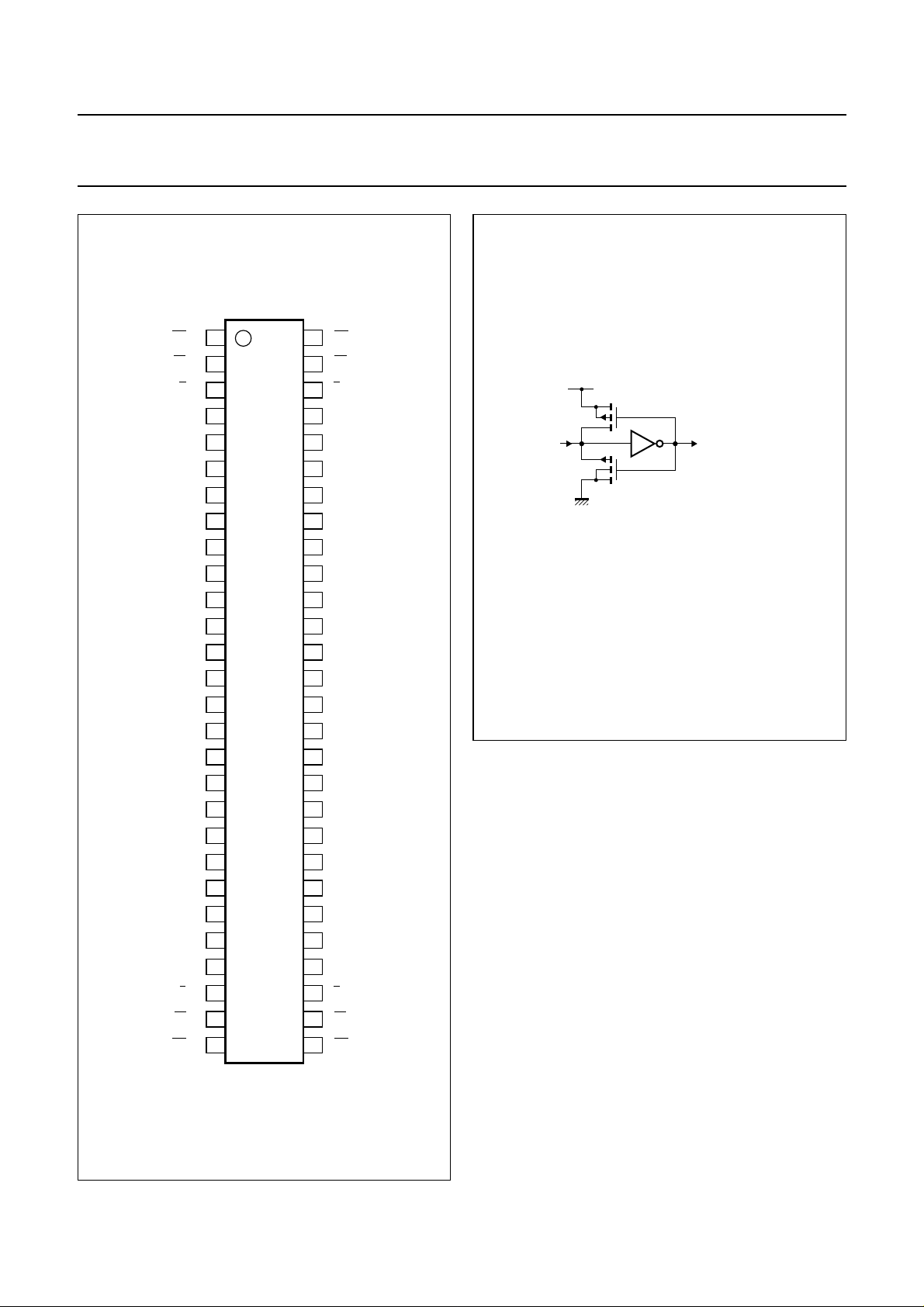
Fig.3 Logic symbol.
handbook, full pagewidth
56
1EN3
54
G1
55
1C5
1
2EN4
3
G2
2
2C6
5
651
8
9
10
12
13
14
6D
3
4
5D
52
49
48
47
45
44
43
Fig.4 IEC logic symbol.
1999 Nov 23 5
29
28
30
31
27
26
15
16 41
17
19
20
21
23
24
EN7[BA
EN8[AB
C9
G10
C11
G12
9
12D
]
]
11D
10
MNA299
42
40
38
37
36
34
33
Philips Semiconductors Product specification
16-bit D-type registered transceiver; 3-state 74ALVCH16543
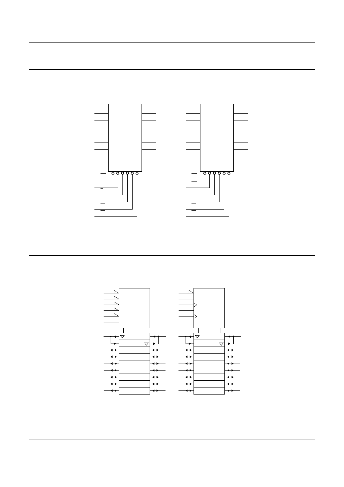
handbook, full pagewidth
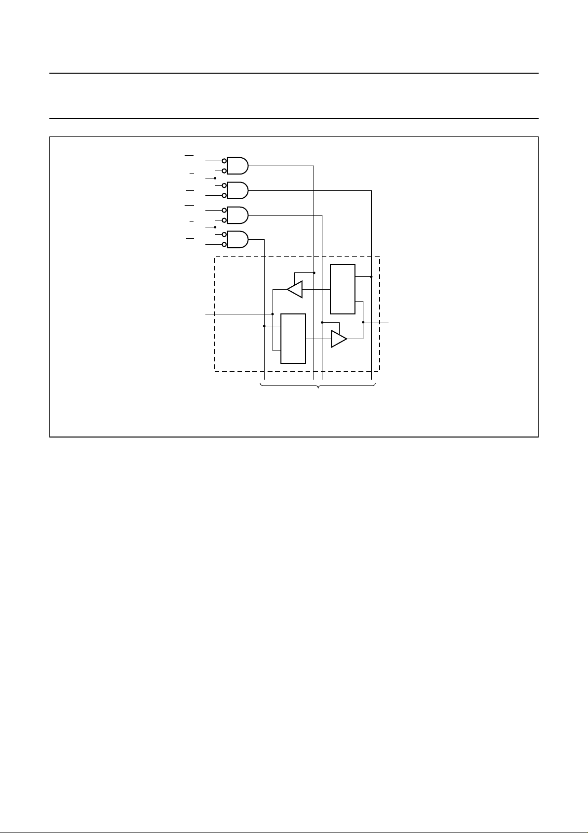
nOE
nE
nLE
nOE
nE
nLE
AB
BA
BA
AB
AB
AB
nA
1
LE
8 IDENTICAL
CHANNELS
D
to 7 other channels
Fig.5 Logic diagram (one section).
LE
D
nB
1
MNA301
1999 Nov 23 6
 Loading...