

Philips 74alvch16500 DATASHEETS

INTEGRATED CIRCUITS
74ALVCH16500
18-bit universal bus transceiver (3-State)
Product specification
Supersedes data of 1998 Aug 31
IC24 Data Handbook
1998 Sep 24
Philips Semiconductors Product specification
1
CPDPower dissi ation ca acitance er latch
V
GND to V
1
F
74AL VCH1650018-bit universal bus transceiver (3-State)
FEA TURES
•Complies with JEDEC standard no. 8-1A
•CMOS low power consumption
•Direct interface with TTL levels
•Current drive ± 24 mA at 3.0 V
•All inputs have bushold circuitry
•Output drive capability 50Ω transmission lines @ 85°C
•MULTIBYTE
•Low inductance multiple V
and ground bounce
TM
flow-through standard pin-out architecture
and ground pins for minimum noise
CC
DESCRIPTION
The 74ALVCH16500 is a high-performance CMOS product.
This device is an 18-bit universal transceiver featuring non-inverting
3-State bus compatible outputs in both send and receive directions.
Data flow in each direction is controlled by output enable (OE
OE
), latch enable (LEAB and LEBA), and clock (CPAB and CPBA)
BA
inputs. For A-to-B data flow, the device operates in the transparent
mode when LE
is held at a High or Low logic level. If LEAB is Low, the A-bus
CP
AB
data is stored in the latch/flip-flop on the High-to-Low transition of
CP
. When OEAB is High, the outputs are active. When OEAB is
AB
Low, the outputs are in the high-impedance state.
Data flow for B-to-A is similar to that of A-to-B but uses OE
and CPBA. The output enables are complimentary (OEAB is active
High, and OE
To ensure the high impedance state during power up or power
down, OE
OE
should be tied to GND through a pulldown resistor; the
AB
minimum value of the resistor is determined by the
current-sinking/current-sourcing capability of the driver.
Active bus-hold circuitry is provided to hold unused or floating data
inputs at a valid logic level.
is High. When LEAB is Low, the A data is latched if
AB
is active Low).
BA
should be tied to VCC through a pullup resistor and
BA
QUICK REFERENCE DATA
GND = 0V; T
SYMBOL PARAMETER CONDITIONS TYPICAL UNIT
= 25°C; tr = tf = 2.5ns
amb
BA
AB
, LE
and
BA
t
PHL/tPLH
C
I/O
C
I
NOTES:
1. C
is used to determine the dynamic power dissipation (PD in µW):
PD
= CPD × V
P
D
= output frequency in MHz; VCC = supply voltage in V; (CL × V
f
o
CC
Propagation delay
An, Bn to Bn, An
Input/output capacitance 8.0 pF
Input capacitance 4.0 pF
2
× fi + (CL × V
p
CC
p
2
× fo) where: fi = input frequency in MHz; CL = output load capacitance in pF;
p
VCC = 2.5V, CL = 30pF
VCC = 3.3V, CL = 50pF
=
I
2
× fo) = sum of outputs.
CC
CC
3.1
2.9
Outputs enabled 21
Outputs disabled 3
ORDERING INFORMATION
PACKAGES TEMPERATURE RANGE OUTSIDE NORTH AMERICA DWG NUMBER
56-Pin Plastic TSSOP Type II –40°C to +85°C 74ALVCH16500 DGG SOT364-1
ns
p
1998 Sep 24 8533-2125 20079
2
Philips Semiconductors Product specification
74ALVCH1650018-bit universal bus transceiver (3-State)
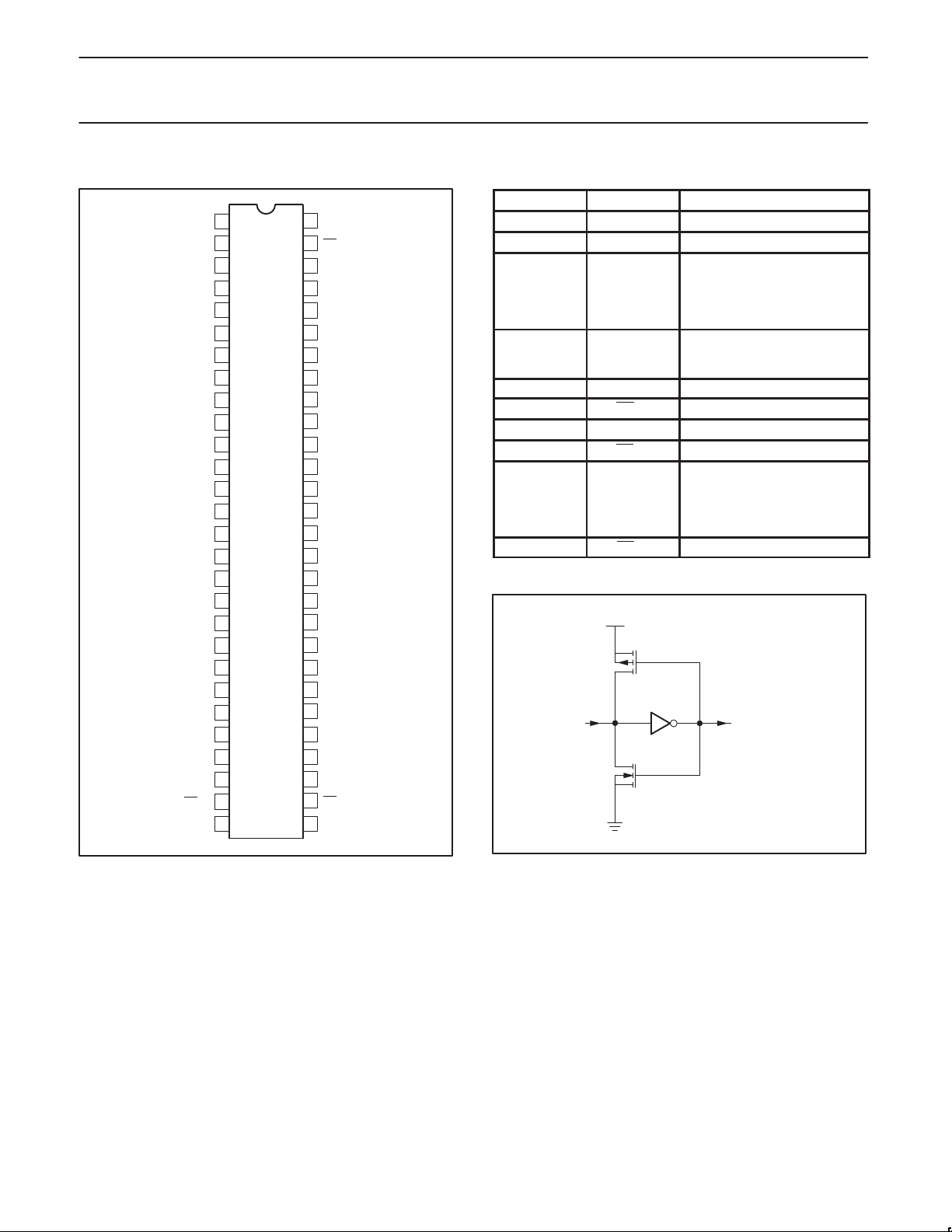
PIN CONFIGURATION
OE
1
AB
LE
2
AB
3
A0
4
GND
5
A1
6
A2
7
V
CC
A3
8
9
A4
10
A5
11
GND
12
A6
13
A7
14
A8
15
A9
16
A10
17
A11
18
GND
19
A12
20
A13
21
A14
22
V
CC
A15
23
A16
24
25
GND
26
A17
27
OE
BA
LE
28
BA
56
55
54
53
52
51
50
49
48
47
46
45
44
43
42
41
40
39
38
37
36
35
34
33
32
31
30
29
SW00080
GND
CP
A0
GND
B1
B2
V
CC
B3
B4
B5
GND
B6
B7
B8
B9
B10
B11
GND
B12
B13
B14
V
CC
B15
B16
GND
B17
CP
GND
PIN DESCRIPTION
PIN NUMBER SYMBOL NAME AND FUNCTION
1 OE
AB
2 LE
AB
AB
Output enable A-to-B
Latch enable A-to-B
3, 5, 6, 8, 9,
10, 12, 13, 14,
15, 16, 17, 19,
A0 to A17 Data inputs/outputs
20, 21, 23, 24,
26
4, 11, 18, 25,
29, 32, 39, 46,
GND Ground (0V)
53, 56
7, 22, 35, 50 V
27 OE
28 LE
30 CP
CC
BA
BA
BA
Positive supply voltage
Output enable B-to-A
Latch enable B-to-A
Clock input B-to-A
54, 52, 51, 49,
48, 47, 45, 44,
43, 42, 41, 40,
B0 to B17 Data inputs/outputs
38, 37, 36, 34,
33, 31
55 CP
AB
Clock input A-to-B
BUS HOLD CIRCUIT
V
CC
Data Input
BA
To internal circuit
SW00044
1998 Sep 24
3
Philips Semiconductors Product specification
74ALVCH1650018-bit universal bus transceiver (3-State)
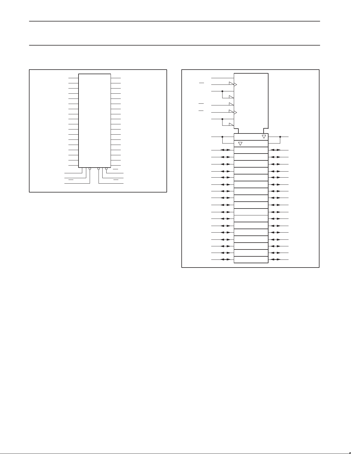
LOGIC SYMBOL
3
5
6
8
9
10
12
13
14
15
16
17
19
20
21
23
24
26
OE
1
LE
2
CP
55
A0
A1
A2
A3
A4
A5
A6
A7
A8
A9
A10
A11
A12
A13
A14
A15
A16
A17
LOGIC SYMBOL (IEEE/IEC)
B0
54
B1
52
B2
51
B3
49
B4
48
B5
47
B6
45
B7
44
B8
43
B9
42
B10
41
B11
40
B12
38
B13
37
B14
36
B15
34
B16
33
B17
31
OE
AB
AB
AB
LE
CP
27
BA
28
BA
30
BA
SW00081
OE
OE
CP
CP
LE
LE
A10
A11
A12
A13
A14
A15
A16
A17
1
AB
56
AB
2
AB
27
AB
30
BA
28
BA
3
A0
5
A1
6
A2
8
A3
9
A4
10
A5
12
A6
13
A7
14
A8
15
A9
16
17
19
20
21
23
24
26
EN1
2C3
C3
G2
EN4
5C6
C6
G5
3D 1 1
416D
54
B0
52
B1
51
B2
49
B3
48
B4
47
B5
45
B6
44
B7
43
B8
42
B9
41
B10
40
B11
38
B12
37
B13
36
B14
34
B15
33
B16
31
B17
SW00082
1998 Sep 24
4
Philips Semiconductors Product specification
Latch data & dis lay
Clock data & dis lay
Hold data & dis lay
74ALVCH1650018-bit universal bus transceiver (3-State)
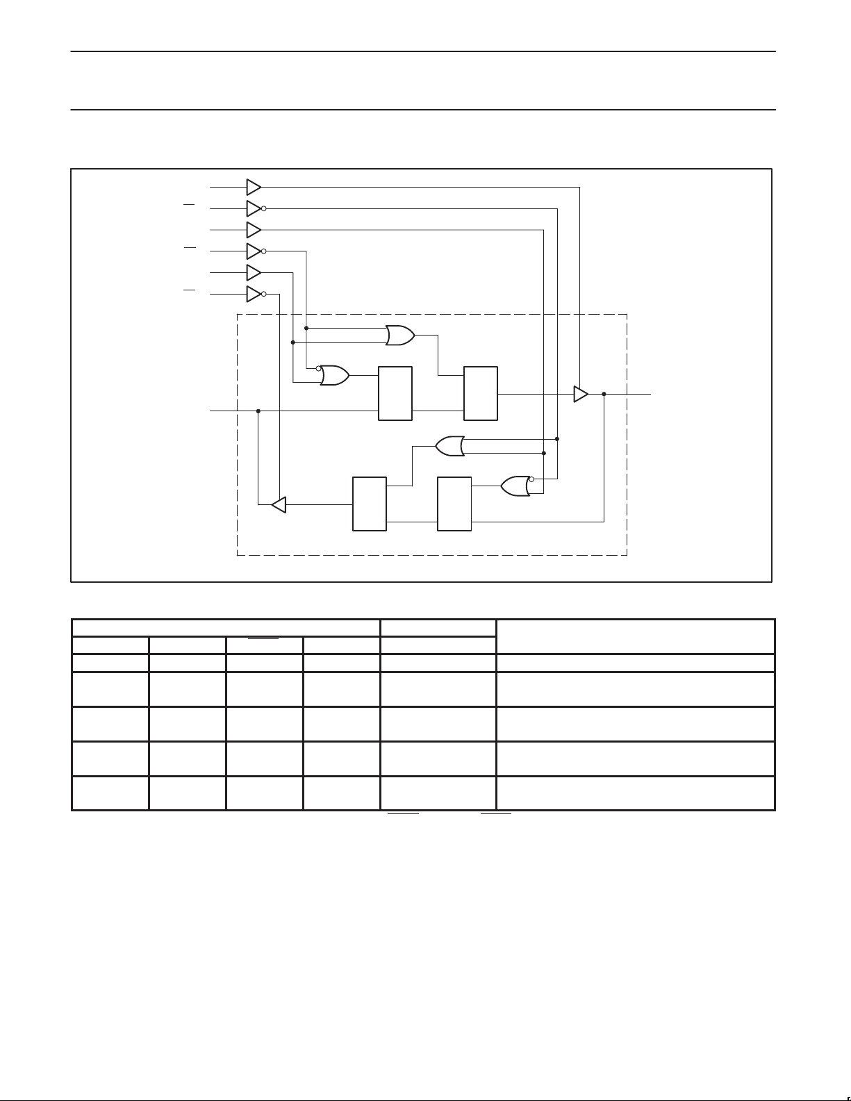
LOGIC DIAGRAM (one section)
OE
AB
CP
BA
LE
BA
CP
AB
LE
AB
OE
BA
C1
An
18 IDENTICAL CHANNELS
1D
C1
1D
C1
1D
C1
1D
FUNCTION TABLE
INPUTS OUTPUTS
OEAB LEAB CPAB An Bn
L H X X Z Disabled
H H X H H
H H X L L
H ↓ X h H
H ↓ X I L
H L ↓ h H
H L ↓ I L
H L H or L X H
H L H or L X L
NOTE: A-to-B data flow is shown; B-to-A flow is similar but uses OEBA, LEBA, and CPBA.
H = High voltage level
h = High voltage level one set-up time prior to the Enable or Clock transition
L = Low voltage level
I = Low voltage level one set-up time prior to the Enable or Clock transition
NC= No Change
X = Don’t care
Z = High Impedance ”off” state
↓ = High-to-Low Enable or Clock transition
Bn
SW00090
OPERATING MODE
Transparent
p
p
p
1998 Sep 24
5
 Loading...