

INTEGRATED CIRCUITS
74ALVCH16374
2.5V/3.3V 16-bit edge-triggered D-type
flip-flop (3-State)
Product specification
Supersedes data of 1997 Mar 21
IC24 Data Handbook
1998 Jun 18
Philips Semiconductors Product specification
t
gy
ns
f
Maximum clock frequenc
CPDPower dissipation capacitance per flip-flop
V
GND to V
1
pF
16-bit edge-triggered D-type flip-flop (3-State)
FEA TURES
•Wide supply voltage range of 1.2 V to 3.6 V
•Complies with JEDEC standard no. 8-1A
•CMOS low power consumption
•MULTIBYTE
•Low inductance multiple V
and ground bounce
TM
flow-through standard pin-out architecture
and ground pins for minimum noise
CC
•Direct interface with TTL levels
•All data inputs have bushold
•Output drive capability 50Ω transmission lines @ 85°C
•Current drive ±24 mA at 3.0 V
DESCRIPTION
The 74ALVCH16374 is a 16-bit edge-triggered flip-flop featuring
separate D-type inputs for each flip-flop and 3-State outputs for bus
oriented applications. Incorporates bus hold data inputs which
eliminate the need for external pull-up or pull-down resistors to hold
unused inputs. The 74AL VCH16374 consists of 2 sections of eight
edge-triggered flip-flops. A clock (CP) input and an output enable
(OE
) are provided per 8-bit section.
The flip-flops will store the state of their individual D-inputs that meet
the set-up and hold time requirements on the LOW-to-HIGH CP
transition.
When OE
outputs. When OE
OFF-state. Operation of the OE
flip-flops.
is LOW, the contents of the flip-flops are available at the
is HIGH, the outputs go to the high impedance
input does not affect the state of the
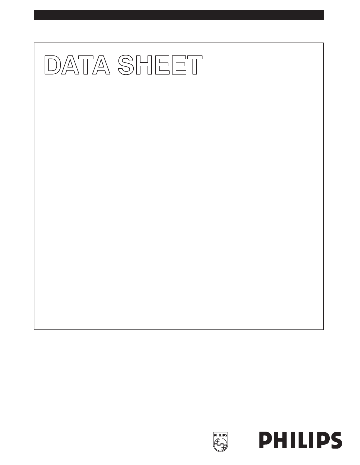
PIN CONFIGURATION
1OE
1Q0
1Q1
GND
1Q2
1Q3
V
1Q4
1Q5
GND
1Q6
1Q7
2Q0
2Q1
GND
2Q2
2Q3
V
2Q4
2Q5
GND
2Q6
2Q7
2OE
74AL VCH16374
48
1
2
3
4
5
6
7
CC
8
9
10
11
12
13
14
15
16
17
18
CC
19
20
21
22
23
24
1CP
47
1D0
46
1D1
45
GND
44
1D2
43
1D3
42
V
CC
41
1D4
40
1D5
39
GND
38
1D6
37
1D7
36
2D0
35
2D1
34
GND
33
2D2
32
2D3
31
V
CC
30
2D4
29
2D5
28
GND
27
2D6
26
2D7
25
2CP
QUICK REFERENCE DA TA
GND = 0V; T
SYMBOL
PHL/tPLH
MAX
C
I
NOTE:
is used to determine the dynamic power dissipation (PD in W):
1. C
PD
= CPD × V
P
D
= output frequency in MHz; VCC = supply voltage in V; (CL × V
f
o
= 25°C; tr = tf ≤ 2.5 ns
amb
Propagation delay
CP to Qn
Input capacitance 5.0 pF
2
× fi + (CL × V
CC
ORDERING INFORMATION
PACKAGES TEMPERATURE RANGE OUTSIDE NORTH AMERICA NORTH AMERICA DWG NUMBER
48-Pin Plastic SSOP Type III –40°C to +85°C 74ALVCH16374 DL ACH16374 DL SOT370-1
48-Pin Plastic TSSOP Type II –40°C to +85°C 74ALVCH16374 DGG ACH16374 DGG SOT362-1
1998 Jun 18 853-2073 19604
SW00074
PARAMETER CONDITIONS TYPICAL UNIT
VCC = 2.5V, CL = 30pF 2.3
VCC = 3.3V, CL = 50pF 2.4
y
p
p
2
× fo) where: fi = input frequency in MHz; CL = output load capacitance in pF;
CC
p
p
VCC = 2.5V 300 MHz
VCC = 3.3V 350 MHz
p
=
I
CC
CC
2
× fo) = sum of outputs.
Outputs enabled 16
Outputs disabled 10
2
p
Philips Semiconductors Product specification
OPERATING MODES
16-bit edge-triggered D-type flip-flop (3-State)
PIN DESCRIPTION
PIN NUMBER SYMBOL NAME AND FUNCTION
1 1OE
2, 3, 5, 6, 8, 9,
11, 12
4, 10, 15, 21,
28, 34, 39, 45
7, 18, 31, 42 V
13, 14, 16, 17,
19, 20, 22, 23
1Q0 to 1Q7 3-State flip-flop outputs
GND Ground (0V)
CC
2Q0 to 2Q7 3-State flip-flop outputs
24 2OE
25 2CP Clock input
36, 35, 33, 32,
30, 29, 27, 26
47, 46, 44, 43,
41, 40, 38, 37
2D0 to 2D7 Data inputs
1D0 to 1D7 Data inputs
48 1CP Clock input
Output enable input
(active LOW)
Positive supply voltage
Output enable input
(active LOW)
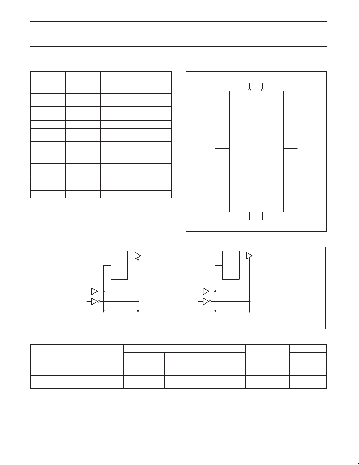
LOGIC SYMBOL
47
46
44
43
41
40
38
37
36
35
33
32
30
29
27
26
1D0
1D1
1D2
1D3
1D4
1D5
1D6
1D7
2D0
2D1
2D2
2D3
2D4
2D5
2D6
2D7
74ALVCH16374
241
1OE 2OE
1CP 2CP
1Q0
1Q1
1Q2
1Q3
1Q4
1Q5
1Q6
1Q7
2Q0
2Q1
2Q2
2Q3
2Q4
2Q5
2Q6
2Q7
2
3
5
6
8
9
11
12
13
14
16
17
19
20
22
23
LOGIC DIAGRAM
1D0
1CP
1OE
DQ
CP
FF1
TO 7 OTHER CHANNELS
1Q0
FUNCTION TABLE
INPUTS
OE CP Dn
Load and read register
Load register and disable outputs
L
L
H
H
H = HIGH voltage level
h = HIGH voltage level one set-up time prior to the HIGH-to-LOW LE transition
L = LOW voltage level
l = LOW voltage level one set-up time prior to the HIGH-to-LOW LE transition
Z = high impedance OFF-state
= LOW-to-HIGH CP transition
2D0
2CP
2OE
48 25
DQ
CP
FF9
TO 7 OTHER CHANNELS
SW00076
l
h
l
h
2Q0
INTERNAL
FLIP-FLOPS
L
H
L
H
SW00075
OUTPUTS
Q0 to Q7
L
H
Z
Z
1998 Jun 18
3
Philips Semiconductors Product specification
SYMBOL
PARAMETER
CONDITIONS
UNIT
V
DC Input voltage range
V
16-bit edge-triggered D-type flip-flop (3-State)
LOGIC SYMBOL (IEEE/IEC)
1
1OE
1CLK
2OE
2CLK
1D0
1D1
1D2
1D3
1D4
1D5
1D6
1D7
2D0
2D1
2D2
2D3
2D4
2D5
2D6
2D7
48
24
25
47
46
44
43
41
40
38
37
36
35
33
32
30
29
27
26
1EN
2EN
1D
C1
C2
2
1 ∇
2 ∇2D
1Q0
3
1Q1
5
1Q2
6
1Q3
8
1Q4
9
1Q5
11
1Q6
12
1Q7
13
2Q0
14
2Q1
16
2Q2
17
2Q3
19
2Q4
20
2Q5
22
2Q6
23
2Q7
SW00199
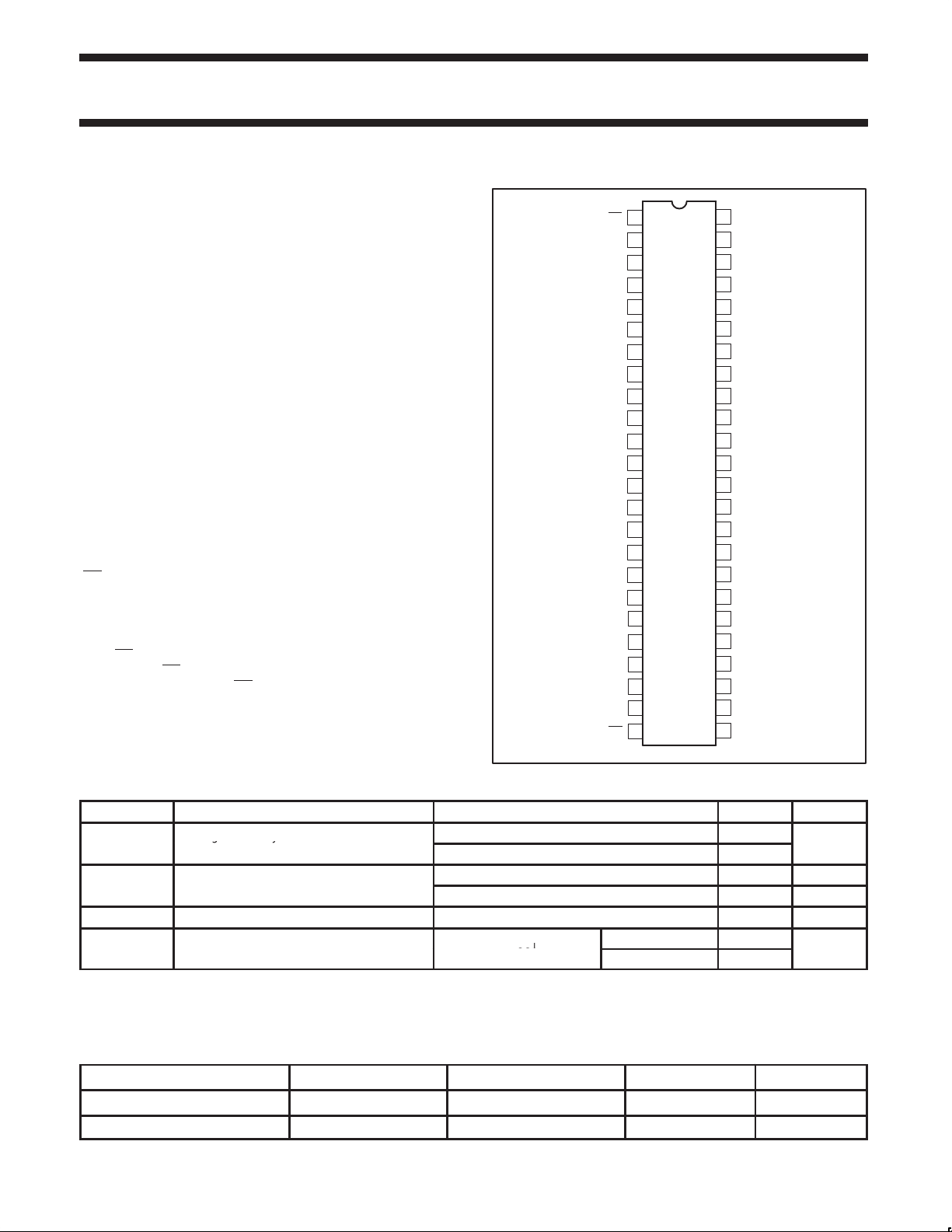
BUS HOLD CIRCUIT
V
CC
Data Input
74ALVCH16374
To internal circuit
SW00044
RECOMMENDED OPERATING CONDITIONS
DC supply voltage 2.5V range (for max. speed
performance @ 30 pF output load)
V
CC
V
O
T
amb
tr, t
DC supply voltage 3.3V range (for max. speed
performance @ 50 pF output load)
DC supply voltage (for low-voltage applications) 1.2 3.6
I
p
DC output voltage range 0 V
Operating free-air temperature range –40 +85 °C
Input rise and fall times
f
LIMITS
MIN MAX
2.3 2.7
3.0 3.6
For data input pins 0 V
For control pins 0 5.5
VCC = 2.3 to 3.0V
VCC = 3.0 to 3.6V
0
0
20
10
CC
CC
V
V
ns/V
1998 Jun 18
4
 Loading...