Philips 74alvc164245 DATASHEETS

INTEGRATED CIRCUITS
74ALVC164245
16-bit dual supply translating transceiver
(3-State)
Product specification
Supersedes data of 1995 Jul 01
IC24 Data Handbook
1998 Aug 26

Philips Semiconductors Product specification
74AL VC16424516-bit dual supply translating transceiver (3-State)
FEA TURES
•Wide supply voltage range
– A port: 1.2 to 3.6V
– B port: 1.2 to 5.5V
•Complies with JEDEC standard no. 8-1A
•Control inputs voltage range from 2.7V to 5.5V
•CMOS low power consumption
•Direct interface with TTL levels
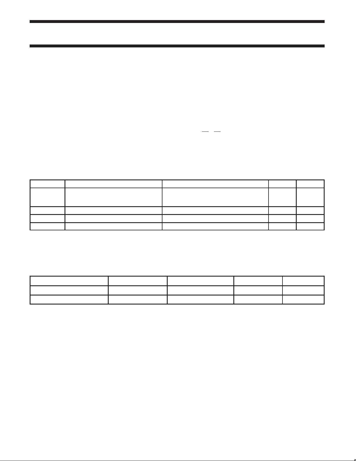
QUICK REFERENCE DATA
GND = 0V; T
SYMBOL
t
PHL/tPLH
C
I
C
I/O
C
PD
NOTES:
is used to determine the dynamic power dissipation (PD in µW):
1. C
PD
= CPD × V
P
D
f
= input frequency in MHz; CL = output load capacity in pF;
i
= output frequency in MHz; VCC = supply voltage in V;
f
o
S (C
= 25°C; tr = tf ≤ 2.5ns
amb
Propagation delay
nA to nB
nB to nA
Input capacitance 5 pF
Input/output capacitance 10 pF
Power dissipation capacitance VI = GND to V
CC
2
× V
L
× fo) = sum of outputs.
CC
2
× fi + S (CL × V
PARAMETER CONDITIONS TYPICAL UNIT
2
× fo) where:
CC
CL = 50pF
V
= 5.0V
CC1
V
= 3.3V
CC2
DESCRIPTION
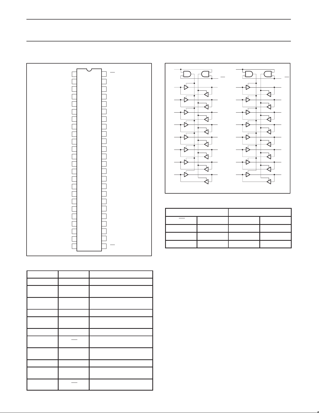
The 74ALVC164245 is a high-performance, low-power, low-voltage,
Si-gate CMOS device, superior to most advanced CMOS
compatible TTL families.
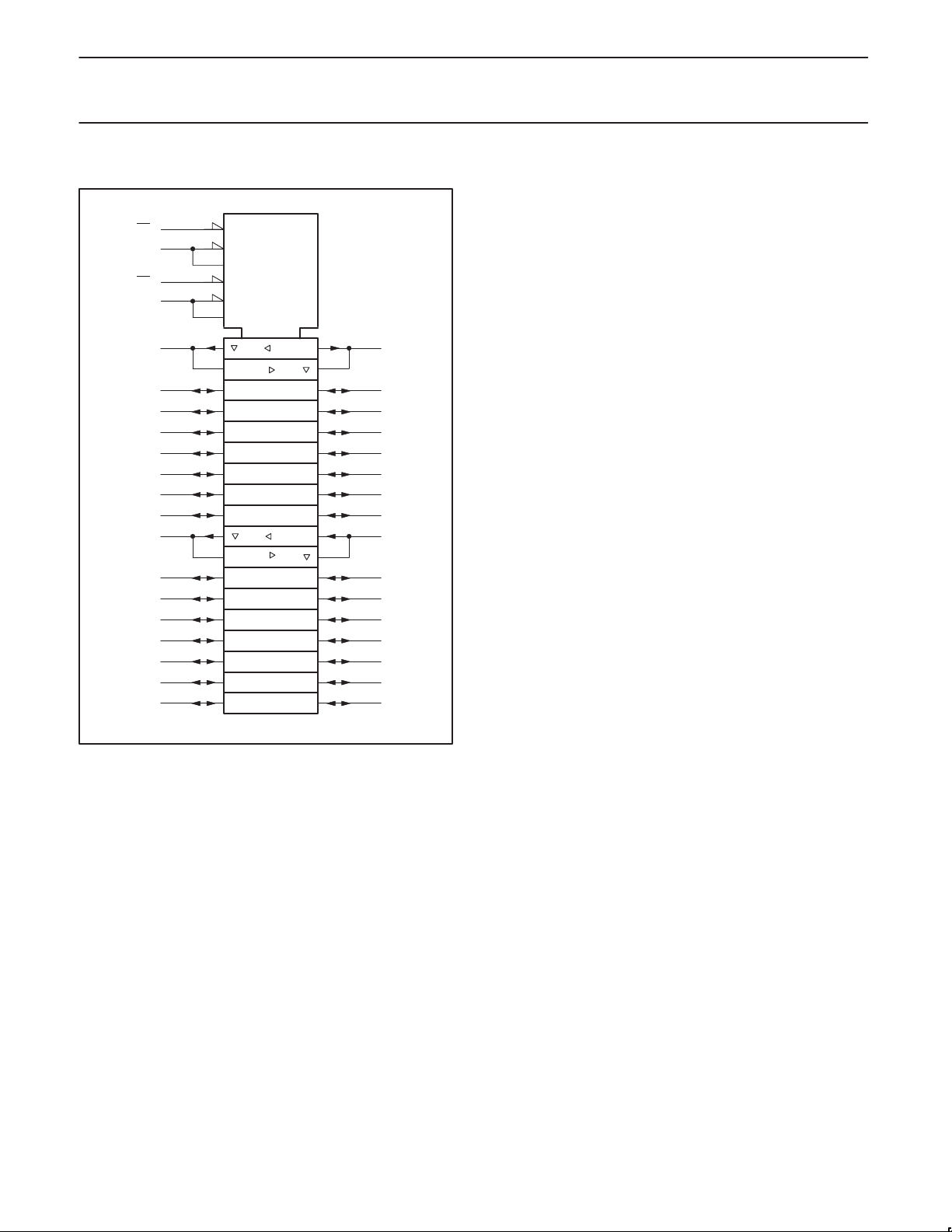
The 74ALVC164245 is a 16-bit (dual-octal) translating transceiver
and is designed to interface between a 5V bus and 3V bus in a
mixed 3V/5V supply environment. This device can be used as two
8-bit transceivers or one 16-bit transceiver. The direction control
inputs (1DIR, 2DIR) determine the direction of the data flow. nDIR
(active HIGH) enables data from nA ports to nB ports. nDIR (active
LOW) enables data from nB ports to nA ports. The output enable
inputs (1OE
placing them in a high impedance OFF-state. The nB ports interface
with the 5V bus. The nA ports interface with the 3V bus. In suspend
mode, when one of the supply voltages is zero, there will be no
current flow from the non zero supply towards the zero supply.
V
CC1
, 2OE), when HIGH, disable both nA and nB ports by
≥ V
(except in suspend mode).
CC2
3.7
3.1
CC
1
20 pF
ns
ORDERING INFORMATION
PACKAGES TEMPERATURE RANGE OUTSIDE NORTH AMERICA NORTH AMERICA DWG NUMBER
48-Pin Plastic SSOP Type III –40°C to +85°C 74ALVC164245 DL AC164245 DL SOT370-1
48-Pin Plastic TSSOP Type II –40°C to +85°C 74ALVC164245 DGG AC164245 DGG SOT362-1
1998 Aug 26 853-21 12 019920
2

Philips Semiconductors Product specification
74ALVC16424516-bit dual supply translating transceiver (3-State)
PIN CONFIGURATION
1OE
SW00198
48
47
1A0
46
1A1
45
GND
44
1A2
43
1A3
42
V
CC2
41
1A4
40
1A5
39
GND
38
1A6
37
1A7
36
2A0
35
2A1
34
GND
33
2A2
32
2A3
31
V
CC2
30
2A4
29
2A5
28
GND
27
2A6
26
2A7
25
2OE
1DIR
1B0
1B1
GND
1B2
1B3
V
CC1
1B4
1B5
GND
1B6
1B7
2B0
2B1
GND
2B2
2B3
V
CC1
2B4
2B5
GND
2B6
2B7
2DIR
1
2
3
4
5
6
7
8
9
10
11
12
13
14
15
16
17
18
19
20
21
22
23
24
PIN DESCRIPTION
PIN NUMBER SYMBOL NAME AND FUNCTION
1 1DIR Direction control
2, 3, 5, 6, 8, 9,
11, 12
4, 10, 15, 21,
28, 34, 39, 45
7, 18 V
13, 14, 16, 17,
19, 20, 22, 23
24 2DIR Direction control
25 2OE
26, 27, 29, 30,
32, 33, 35, 36
31, 42 V
37, 38, 40, 41,
43, 44, 46, 47
48 1OE
1B0 to 1B7 Data inputs/outputs
GND GND
CC1
Positive supply voltage (5V bus)
2B0 to 2B7 Data inputs/outputs
Output enable input
(active LOW)
2A7 to 2A0 Data inputs/outputs
CC2
Positive supply voltage (3V bus)
1A7 to 1A0 Data inputs/outputs
Output enable input
(active LOW)
LOGIC SYMBOL
1
1DIR
47
1A0
46
1A1
44
1A2
43
1A3
41
1A4
40
1A5
38
1A6
37 12
1A7
48
1OE
2
1B0
3
1B1
5
1B2
6
1B3
8
1B4
9
1B5
11
1B6
1B7
24
2DIR
36
2A0
35
2A1
33
2A2
32
2A3
30
2A4
29
2A5
27
2A6
26 23
2A7
FUNCTION TABLE
INPUTS OUTPUTS
nOE nDIR nAn nBn
L L A = B inputs
L H inputs B = A
H X Z Z
H = HIGH voltage level
L = LOW voltage level
X = don’t care
Z = high impedance OFF-state
25
2OE
13
2B0
14
2B1
16
2B2
17
2B3
19
2B4
20
2B5
22
2B6
2B7
SW00197
1998 Aug 26
3

Philips Semiconductors Product specification
74ALVC16424516-bit dual supply translating transceiver (3-State)
LOGIC SYMBOL (IEEE/IEC)
1OE
1DIR
2OE
2DIR
1A0
1A1
1A2
1A3
1A4
1A5
1A6
1A7
2A0
2A1
2A2
2A3
2A4
2A5
2A6
2A7
48
1
25
24
47
46
44
43
41
40
38
37
36
35
33
32
30
29
27
26
G3
3 EN1 [BA]
3 EN2 [AB]
G6
6 EN4 [BA]
6 EN5 [AB]
1
4
2
1B0
2
5
3
1B1
5
1B2
6
1B3
8
1B4
9
1B5
11
1B6
12
1B7
13
2B0
14
2B1
16
2B2
17
2B3
19
2B4
20
2B5
22
2B6
23
2B7
SW00196
1998 Aug 26
4
 Loading...