

Philips 74ALVC16244DL, 74ALVC16244DGG, 74ALVCH16244DL, 74ALVCH16244DGG Datasheet

INTEGRATED CIRCUITS
74ALVC16244/74ALVCH16244
2.5V/3.3V 16-bit buffer/line driver (3-State)
Product specification
Supersedes data of 1997 Mar 21
IC24 Data Handbook
1998 Jun 29
Philips Semiconductors Product specification
CPDPower dissipation capacitance per buffer
V
GND to V
1
pF
16-bit buffer/line driver (3-State)
FEA TURES
•Wide supply voltage range of 1.2V to 3.6V
•Complies with JEDEC standard no. 8-1A
•CMOS low power consumption
•MULTIBYTE
•Low inductance multiple V
and ground bounce
•Direct interface with TTL levels
•Bus hold on data inputs (74ALVCH16244 only)
•Output drive capability 50Ω transmission lines @ 85°C
•Current drive ±24 mA at 3.0 V
DESCRIPTION
The 74ALVC16244(74ALVCH16244) is a 16-bit non-inverting
buffer/line driver with 3-State outputs. The device can be used as
four 4-bit buffers, two 8-bit buffers or one 16-bit buffer. The 3-State
outputs are controlled by the output enable inputs 1OE
HIGH on nOE
OFF-state.
The 74ALVCH16244 has active bus hold circuitry which is provided
to hold unused or floating data inputs at a valid logic level. This
feature eliminates the need for external pull-up or pull-down
resistors.
The 74ALVC16244 has 5V tolerant inputs.
QUICK REFERENCE DA TA
GND = 0 V; T
SYMBOL
t
PHL/tPLH
C
I
NOTE:
1. C
PD
= CPD × V
P
D
= output frequency in MHz; VCC = supply voltage in V; (CL × V
f
o
TM
flow-through standard pin-out architecture
and GND pins for minimum noise
CC
and 2OE. A
causes the outputs to assume a high impedance
= 25°C; tr = tf ≤ 2.5 ns
amb
PARAMETER CONDITIONS TYPICAL UNIT
Propagation delay
An to Yn
Input capacitance 5.0 pF
p
is used to determine the dynamic power dissipation (PD in W):
2
× fi + (CL × V
CC
p
2
× fo) where: fi = input frequency in MHz; CL = output load capacitance in pF;
CC
p
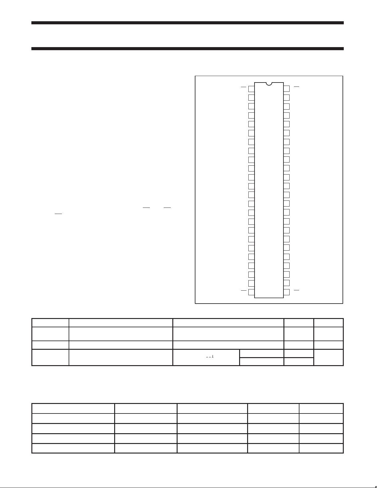
PIN CONFIGURATION
VCC = 2.5V, CL = 30pF
VCC = 3.3V, CL = 50pF
=
I
CC
CC
2
× fo) = sum of the outputs.
74AL VC16244/
74AL VCH16244
1OE
1
2
1Y0
3
1Y1
4
GND
5
1Y2
6
1Y3
7
V
CC
8
2Y0
9
2Y1
10
GND
11
2Y2
12
2Y3
13
3Y0
14
3Y1
15
GND
16
3Y2
17
3Y3
18
V
CC
19
4Y0
20
4Y1
21
GND
22
4Y2
23
4Y3
24
4OE
Outputs enabled 25
Outputs disabled 4
48
47
46
45
44
43
42
41
40
39
38
37
36
35
34
33
32
31
30
29
28
27
26
25
SW00194
2OE
1A0
1A1
GND
1A2
1A3
V
CC
2A0
2A1
GND
2A2
2A3
3A0
3A1
GND
3A2
3A3
V
CC
4A0
4A1
GND
4A2
4A3
3OE
1.9
1.9
ns
p
ORDERING INFORMATION
PACKAGES TEMPERATURE RANGE OUTSIDE NORTH AMERICA NORTH AMERICA DWG NUMBER
48-Pin Plastic SSOP Type III –40°C to +85°C 74ALVC16244 DL AC16244 DL SOT370-1
48-Pin Plastic TSSOP Type II –40°C to +85°C 74ALVC16244 DGG AC16244 DGG SOT362-1
48-Pin Plastic SSOP Type III –40°C to +85°C 74ALVCH16244 DL ACH16244 DL SOT370-1
48-Pin Plastic TSSOP Type II –40°C to +85°C 74ALVCH16244 DGG ACH16244 DGG SOT362-1
1998 Jun 29 853-2082 19638
2
Philips Semiconductors Product specification
16-bit buffer/line driver (3-State)
PIN DESCRIPTION
PIN NUMBER SYMBOL NAME AND FUNCTION
1 1OE
2, 3, 5, 6 1Y0 to 1Y3 Data outputs
4, 10, 15, 21,
28, 34, 39, 45
7, 18, 31, 42 V
GND Ground (0V)
CC
8, 9, 11, 12 2Y0 to 2Y3 Data outputs
13, 14, 16, 17 3Y0 to 3Y3 Data outputs
19, 20, 22, 23 4Y0 to 4Y3 Data outputs
24 4OE
25 3OE
30, 29, 27, 26 4A0 to 4A3 Data inputs
36, 35, 33, 32 3A0 to 3A3 Data inputs
41, 40, 38, 37 2A0 to 2A3 Data inputs
47, 46, 44, 43 1A0 to 1A3 Data inputs
48 2OE
LOGIC SYMBOL
1A0
1A1
1A2
1A3
1OE
2A0
2A1
2A2
47
46
44
43
1
41
40
38
2
3
5
6
8
9
11
Output enable input
(active LOW)
Positive supply voltage
Output enable input
(active LOW)
Output enable input
(active LOW)
Output enable input
(active LOW)
36
3A0
1Y0
35
3A1
1Y1
33
3A2
1Y2
32
3A3
1Y3
25
3OE
30
4A0
2Y0
29
4A1
2Y1
27
4A2
2Y2
13
14
16
17
19
20
22
3Y0
3Y1
3Y2
3Y3
4Y0
4Y1
4Y2
FUNCTION TABLE
INPUTS OUTPUT
nOE nAn nYn
L L L
L H H
H X Z
H = HIGH voltage level
L = LOW voltage level
X = don’t care
Z = high impedance OFF-state
LOGIC SYMBOL (IEEE/IEC)
1OE
2OE
3OE
4OE
1A0
1A1
1A2
1A3
2A0
2A1
2A2
2A3
3A0
3A1
3A2
3A3
4A0
4A1
4A2
4A3
1
48
25
24
47
46
44
43
41
40
38
37
36
35
33
32
30
29
27
26
1EN
2EN
3EN
4EN
BUS HOLD CIRCUIT
V
CC
74ALVC16244/
74ALVCH16244
2
1 ∇
1
2 ∇
1
3 ∇
1
4 ∇
1
1Y0
3
1Y1
5
1Y2
6
1Y3
8
2Y0
9
2Y1
11
2Y2
12
2Y3
13
3Y0
14
3Y1
16
3Y2
17
3Y3
19
4Y0
20
4Y1
22
4Y2
23
4Y3
SW00056
37
2A3
48
2OE
1998 Jun 29
12
2Y3
4A3
4OE
26
24
23
4Y3
SW00195
Data Input
To internal circuit
SW00044
3
 Loading...