

Philips 74ALS623AN, 74ALS623A-1N, 74ALS623A-1D, 74ALS620AN, 74ALS620A-1N Datasheet
...
INTEGRATED CIRCUITS
74ALS620A/74ALS620A–1
74ALS623A/74ALS623A–1
Transceivers
Product specification
IC05 Data Handbook
1991 Feb 08
Philips Semiconductors Product specification
T ransceivers
74ALS620A/74ALS620A-1
74ALS623A/74ALS623A-1
74ALS620A/74ALS620A-1 Octal bus transceiver, inverting (3-State)
74ALS623A/74ALS623A-1 Octal bus transceiver, non-inverting (3-State)
FEA TURES
•Octal bidirectional bus interface
•3-State buffer outputs sink 24mA and source 15mA
•The -1 version sinks 48mA I
TYPE
74ALS620A/620A-1 4.0ns 33mA
74ALS623A/623A-1 4.0ns 38mA
ORDERING INFORMATION
DESCRIPTION
20-pin plastic DIP
20-pin plastic SOL
74ALS620AN, 74ALS620A-1N
74ALS623AN, 74ALS623A-1N
74ALS620AD, 74ALS620A-1D
74ALS623AD, 74ALS623A-1D
within the +5% VCC range
OL
TYPICAL
PROPAGATION
SUPPLY CURRENT
DELA Y
ORDER CODE
COMMERCIAL RANGE
V
= 5V ±10%,
CC
T
= 0°C to +70°C
amb
TYPICAL
(TOTAL)
DRAWING
NUMBER
SOT146-1
SOT163-1
DESCRIPTION
The 74ALS620A and 74ALS623A are octal transceiver featuring
3-State bus compatible outputs in both transmit and receive
directions. The 74ALS620A is an inverting version of the
74ALS623A. The outputs are capable of sinking 24mA and sourcing
up to 15mA, providing very good capacitive drive characteristics.
The outputs for the 74ALS620A-1 and 74ALS623A are capable of
sinking up to 48mA when within the ±5% V
These octal bus transceivers are designed for asynchronous
two-way communication between data buses. The control function
implementation allows for maximum flexibility in timing.
These devices allow data transmission from the A bus to the B bus
or from B bus to A bus, depending on the logic levels at the enable
inputs (OEBA
the device so that the buses are effectively isolated. The
dual-enable configuration gives the 74ALS620A and 74ALS623A the
capability to store data by the simultaneous enabling of OEBA
OEAB. Each output reinforces its input in this transceiver
configuration. Thus when both control inputs are enabled and all
other data sources to the two sets of the bus lines are at high
impedance, both sets of the bus lines (16 in all) will remain at their
last states.
and OEAB). The enable inputs can be used to disable
CC
range.
and
INPUT AND OUTPUT LOADING AND FAN-OUT TABLE
PINS DESCRIPTION
74ALS (U.L.)
HIGH/LOW
A0 – A7, B0 – B7 Data inputs 1.0/1.0 20µA/0.1mA
OEBA, OEAB Output Enable inputs 1.0/1.0 20µA/0.1mA
A0 – A7, B0 – B7 Data outputs 750/240 15mA/24mA
A0 – A7, B0 – B7 Data outputs (-1 version) 750/480 15mA/48mA
NOTE: One (1.0) ALS unit load is defined as: 20µA in the High state and 0.1mA in the Low state.
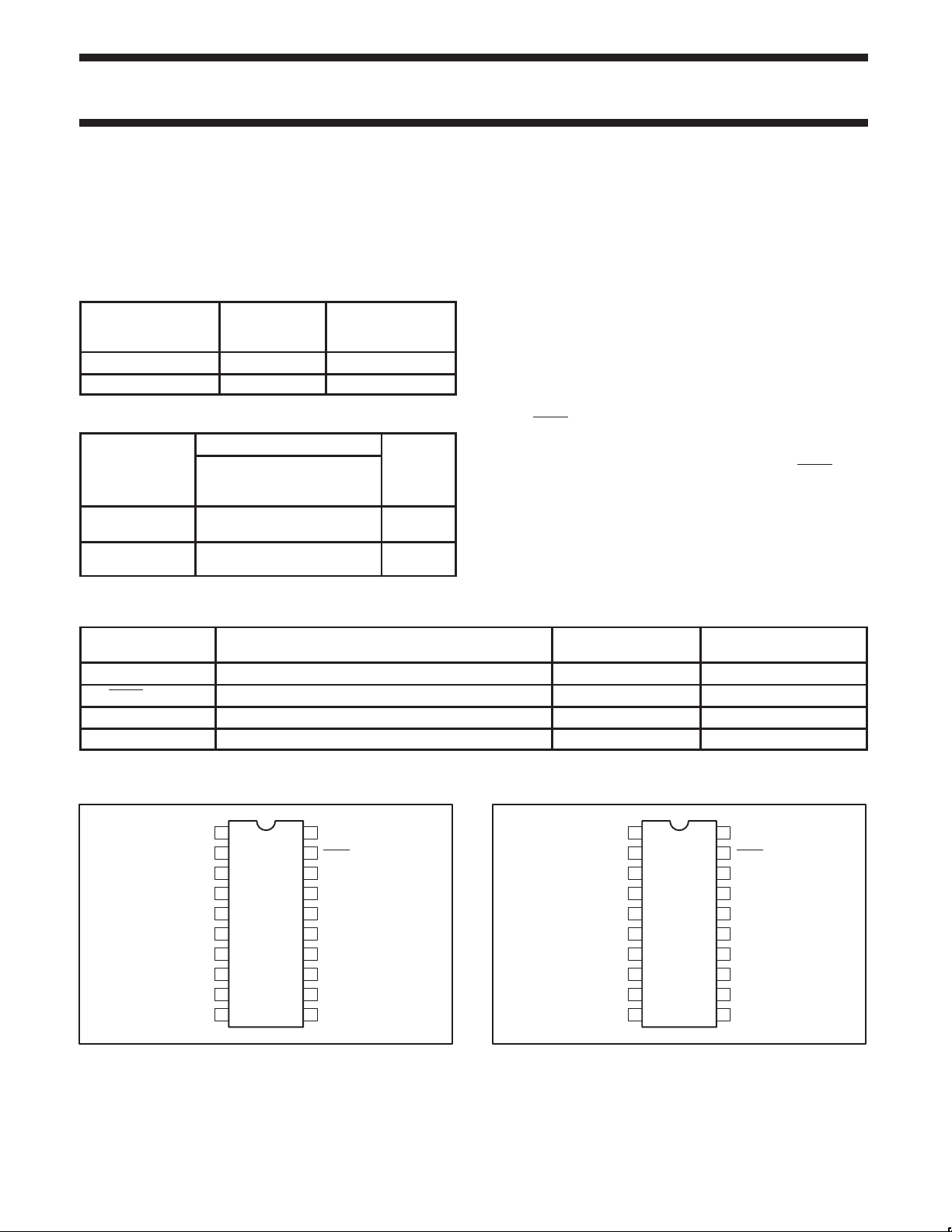
PIN CONFIGURATION – 74ALS620A/74ALS620A-1
1
2
A0
3
A1
4
A2
5
A3
6
A4
7
A5
8
A6
9
A7
10 11
GND
V
20OEAB
CC
19
OEBA
18
B0
17
B1
16
B2
15
B3
14
B4
13
B5
12
B6
B7
SC00101
PIN CONFIGURATION – 74ALS623A/74ALS623A-1
1
2
A0
3
A1
4
A2
5
A3
6
A4
7
A5
8
A6
9
A7
10 11
GND
LOAD VALUE
HIGH/LOW
V
20OEAB
CC
19
OEBA
18
B0
17
B1
16
B2
15
B3
14
B4
13
B5
12
B6
B7
SC00102
1991 Feb 08 853–0020 01670
2

Philips Semiconductors Product specification
Transceivers
LOGIC SYMBOL – 74ALS620A/74ALS620A-1
23456789
A0 A1 A2 A3 A4 A5 A6 A7
1
19
VCC = Pin 20
GND = Pin 10
IEC/IEEE SYMBOL – 74ALS620A/74ALS620A-1
OEAB
OEBA
B0 B1 B2 B3 B4 B5 B6 B7
18 17 16 15 14 13 12 11
SC00103
1
19
EN1
EN2
74ALS620A/74ALS620A-1
74ALS623A/74ALS623A-1
LOGIC SYMBOL – 74ALS623A/74ALS623A-1
23456789
A0 A1 A2 A3 A4 A5 A6 A7
1
19
VCC = Pin 20
GND = Pin 10
IEC/IEEE SYMBOL – 74ALS623A/74ALS623A-1
OEAB
OEBA
B0 B1 B2 B3 B4 B5 B6 B7
18 17 16 15 14 13 12 11
SC00104
1
19
EN1
EN2
2 18
3 17
4 16
5 15
6 14
7 13
8 12
9 11
1
2
SC00105
2 18
3 17
4 16
5 15
6 14
7 13
8 12
9 11
1
2
SC00106
1991 Feb 08
3

Philips Semiconductors Product specification
Transceivers
LOGIC DIAGRAM – 74ALS620A/74ALS620A-1
19
OEBA
1
OEAB
2
A0
3
A1
4
A2
5
A3
6
A4
18
B0
17
B1
16
B2
15
B3
14
B4
74ALS620A/74ALS620A-1
74ALS623A/74ALS623A-1
LOGIC DIAGRAM – 74ALS623A/74ALS623A-1
19
OEBA
1
OEAB
2
A0
3
A1
4
A2
5
A3
6
A4
18
B0
17
B1
16
B2
15
B3
14
B4
7
A5
8
A6
9
A7
VCC = Pin 20
GND = Pin 10
FUNCTION TABLE
INPUTS OPERATING MODES
OEBA OEAB 74ALS620A 74ALS623A
L L B data to A Bus B data to A Bus
L H A data to B Bus A data to B Bus
H L Z Z
L H B data to A Bus B data to A Bus
L H A data to B Bus A data to B Bus
H = High voltage level
L = Low voltage level
X = Don’t care
Z = High impedance “off” state
13
B5
12
B6
11
B7
VCC = Pin 20
SC00107
GND = Pin 10
7
A5
8
A6
9
A7
13
B5
12
B6
11
B7
SC00108
1991 Feb 08
4
 Loading...