Philips 74als377 DATASHEETS

INTEGRATED CIRCUITS
74ALS377
Octal D flip–flop with enable
Product specification
IC05 Data Handbook
1991 Feb 08

Philips Semiconductors Product specification
74ALS377Octal D flip-flop with enable
FEA TURES
•Ideal for addressable register applications
•Enable for address and data synchronization applications
•Eight edge-triggered D-type flip-flops
•Buffered common clock
•See 74ALS273 for master reset version
•See 74ALS373 for transparent latch version
•See 74ALS374 for 3-State version
DESCRIPTION
The 74ALS377 has eight edge-triggered D-type flip-flops with
individual D inputs and Q outputs. The common buffered clock (CP)
input loads all flip-flops simultaneously when the Enable (E
The register is fully edge-triggered. The state of each D input, one
setup time before the Low-to-High clock transition, is transferred to
the corresponding flip-flop’s Q output. The E
input must be stable
one setup time prior to the Low-to-High clock transition for
predictable operation.
TYPE
TYPICAL f
MAX
SUPPLY CURRENT
74ALS377 95MHz 15mA
) is Low.
TYPICAL
(TOTAL)
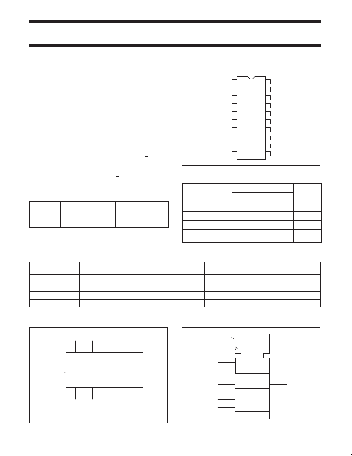
PIN CONFIGURATION
E
1
2
Q0
3
D0
4
D1
5
Q1
6
Q2
7
D2
8
D3
9
Q3
GND
10 11
V
20
CC
19
Q7
18
D7
17
D6
16
Q6
15
Q5
14
D5
13
D4
12
Q4
CP
ORDERING INFORMA TION
ORDER CODE
DESCRIPTION COMMERCIAL RANGE
V
= 5V ±10%,
CC
T
= 0°C to +70°C
amb
20-pin plastic DIP 74ALS377N SOT146-1
20-pin plastic SOL 74ALS377D SOT163-1
20-pin plastic SSOP
Type II
74ALS377DB SOT339-1
DRAWING
NUMBER
SF00350
INPUT AND OUTPUT LOADING AND FAN-OUT TABLE
PINS DESCRIPTION
D0 – D7 Data inputs 1.0/2.0 20µA/0.2mA
CP Clock pulse input (active rising edge) 1.0/1.0 20µA/0.1mA
E Latch enable input 1.0/1.0 20µA/0.1mA
Q0 – Q7 Data outputs 130/240 2.6mA/24mA
NOTE: One (1.0) ALS unit load is defined as: 20µA in the High state and 0.1mA in the Low state.
LOGIC SYMBOL
11
1
V
= Pin 20
CC
GND = Pin 10
CP
E
3 4 7 8 13 14 1817
D0 D1 D2 D3 D4 D5 D6 D7
Q0 Q1 Q2 Q3 Q4 Q5 Q6 Q7
2 5 6 9 12 15 16 19
SF00351
IEC/IEEE SYMBOL
74ALS (U.L.)
HIGH/LOW
1
G1
11
32
4
7
8
13
14
17
18
1C2
2D
LOAD VALUE
HIGH/LOW
5
6
9
12
15
16
19
SF00352
1991 Feb 08 853–1399 01670
2

Philips Semiconductors Product specification
OPERATING MODE
Hold (do nothing)
74ALS377Octal D flip-flop with enable
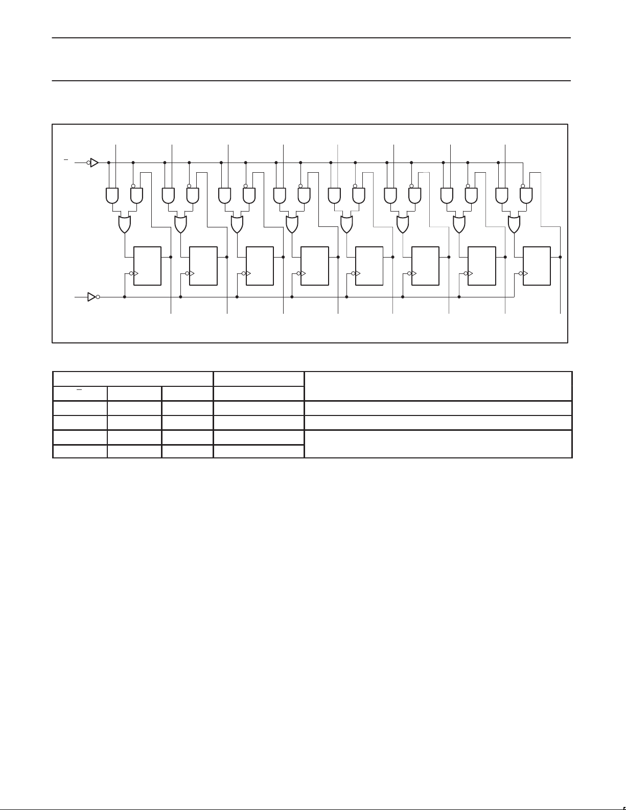
LOGIC DIAGRAM
1
E
11
CP
VCC = Pin 20
GND = Pin 10
D0 D1 D2 D3
3478
DQ
CP
D
CP
2 5 6 9 12 15 16 19
Q0 Q1 Q2 Q3
D
QQ
CP
D4 D5 D6 D7
13 14 17 18
DQ
CP
DQ
FUNCTION TABLE
INPUTS OUTPUTS
E CP Dn Qn
l ↑ h H Load “1”
l ↑ l L Load “0”
h ↑ X NC
H X X NC
H = High-voltage level
h = High state must be present one setup time before the Low-to-High clock transition
L = Low-voltage level
l = Low state must be present one setup time before the Low-to-High clock transition
NC= No change
X = Don’t care
↑ = Low-to-High clock transition
D
CP
CP
Q4 Q5 Q6 Q7
D
QQ
CP
DQ
CP
SF00353
1991 Feb 08
3
 Loading...