

Philips 74als32 DATASHEETS

INTEGRATED CIRCUITS
74ALS32
Quad 2-Input OR gate
Product specification 1991 Feb 08
IC05 Data Handbook
Philips Semiconductors Product specification
74ALS32Quad 2-input OR gate
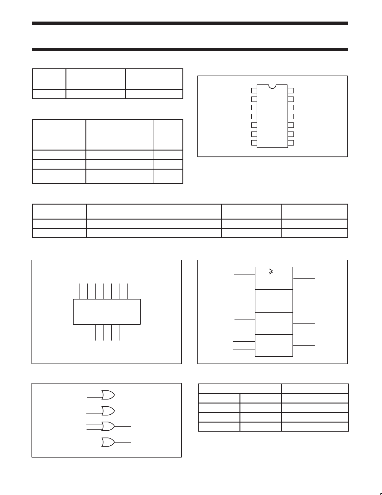
PIN CONFIGURATION
TYPE
TYPICAL
PROPAGATION DELAY
TYPICAL
SUPPLY CURRENT
(TOTAL)
74ALS32 5.0ns 2.3mA
ORDERING INFORMATION
ORDER CODE
DESCRIPTION COMMERCIAL RANGE
V
= 5V ±10%,
CC
T
= 0°C to +70°C
amb
DRAWING
NUMBER
GND 3Y
14-pin plastic DIP 74ALS32N SOT27-1
14-pin plastic SO 74ALS32D SOT108-1
14-pin plastic SSOP
Type II
74ALS32DB SOT337-1
INPUT AND OUTPUT LOADING AND FAN-OUT TABLE
PINS DESCRIPTION
nA, nB Data inputs 1.0/1.0 20µA/0.1mA
nY Data output 20/80 0.4mA/8mA
NOTE: One (1.0) ALS unit load is defined as: 20µA in the High state and 0.1mA in the Low state.
74ALS (U.L.)
HIGH/LOW
11A
2
1B
3
1Y
4
2A
5
2B
6
2Y
14
V
CC
13
4B
12
4A
11
4Y
10
3B
9
3A
87
SC00010
LOAD VALUE
HIGH/LOW
LOGIC SYMBOL
1A 1B 2A 2B 3A 3B 4A 4B
VCC = Pin 14
GND = Pin 7
LOGIC DIAGRAM
VCC = Pin 14
GND = Pin 7
12459101213
1Y 2Y 3Y 4Y
36811
1
1A
2
1B
4
2A
5
2B
9
3A
10
3B
12
4A
13
4B
3
1Y
6
2Y
8
3Y
11
4Y
SC00011
SC00033
IEC/IEEE SYMBOL
1
2
4
5
9
10
12
13
1
FUNCTION TABLE
INPUTS OUTPUT
nA nB nY
H X H
X H H
L L L
H = High voltage level
L = Low voltage level
X = Don’t care
3
6
8
11
SF00041
1991 Feb 08 853–0865 01670
2
Philips Semiconductors Product specification
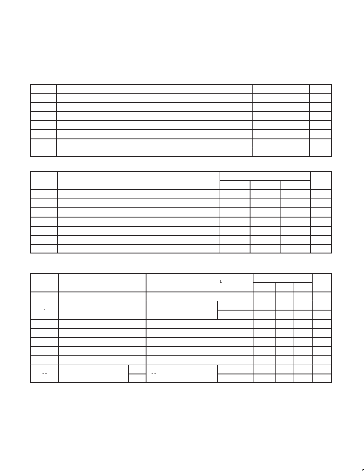
SYMBOL
PARAMETER
UNIT
SYMBOL
PARAMETER
TEST CONDITIONS
1
UNIT
VOLLow-level output voltage
CC
,
IL
,
ICCSupply current (total)
V
MAX
74ALS32Quad 2-input OR gate
ABSOLUTE MAXIMUM RATINGS
(Operation beyond the limit set forth in this table may impair the useful life of the device.
Unless otherwise noted these limits are over the operating free air temperature range.)
SYMBOL
V
V
V
I
OUT
I
OUT
T
amb
T
Supply voltage –0.5 to +7.0 V
CC
Input voltage –0.5 to +7.0 V
IN
Input current –30 to +5 mA
IN
Voltage applied to output in High output state –0.5 to V
Current applied to output in Low output state 16 mA
Operating free air temperature range 0 to +70 °C
Storage temperature range –65 to +150 °C
stg
RECOMMENDED OPERATING CONDITIONS
V
V
V
I
I
OH
I
OL
T
amb
Supply voltage 4.5 5.0 5.5 V
CC
High–level input voltage 2.0 V
IH
Low–level input voltage 0.8 V
IL
Input clamp current –18 mA
Ik
High–level output current –0.4 mA
Low–level output current 8 mA
Operating free air temperature range 0 +70 °C
PARAMETER RATING UNIT
CC
V
LIMITS
MIN NOM MAX
DC ELECTRICAL CHARACTERISTICS
(Over recommended operating free-air temperature range unless otherwise noted.)
LIMITS
MIN TYP2MAX
V
V
I
I
I
High-level output voltage VCC±10%, VIL = MAX, VIH = MIN, IOH = –0.4mA V
OH
I
= 4mA 0.25 0.40 V
p
Input clamp voltage VCC = MIN, II = I
IK
I
Input current at maximum input voltage VCC = MAX, VI = 7.0V 0.1 mA
I
High–level input current VCC = MAX, VI = 2.7V 20 µA
IH
Low–level input current VCC = MAX, VI = 0.5V –0.1 mA
IL
O
Output current
3
pp
VCC = MIN, VIL = MAX,
VIH = MIN
IK
VCC = MAX, VO = 2.25V –30 –112 mA
I
CCH
I
CCL
CC
=
OL
I
= 8mA 0.35 0.50 V
OL
VI = 4.5V 1.6 4.0 mA
VI = GND 2.8 4.9 mA
NOTES:
1. For conditions shown as MIN or MAX, use the appropriate value specified under recommended operating conditions for the applicable type.
2. All typical values are at V
3. The output conditions have been chosen to produce a current that closely approximate one half of the true short–circuit output current, I
CC
= 5V, T
amb
= 25°C.
– 2 V
CC
–0.73 –1.5 V
OS
.
1991 Feb 08
3
 Loading...