

Philips 74als112a DATASHEETS
INTEGRATED CIRCUITS
74ALS112A
Dual J-K negative edge-triggered flip-flop
Product specification 1996 June 27
IC05 Data Handbook
Philips Semiconductors Product specification
74ALS1 12ADual J-K negative edge-triggered flip-flop
DESCRIPTION
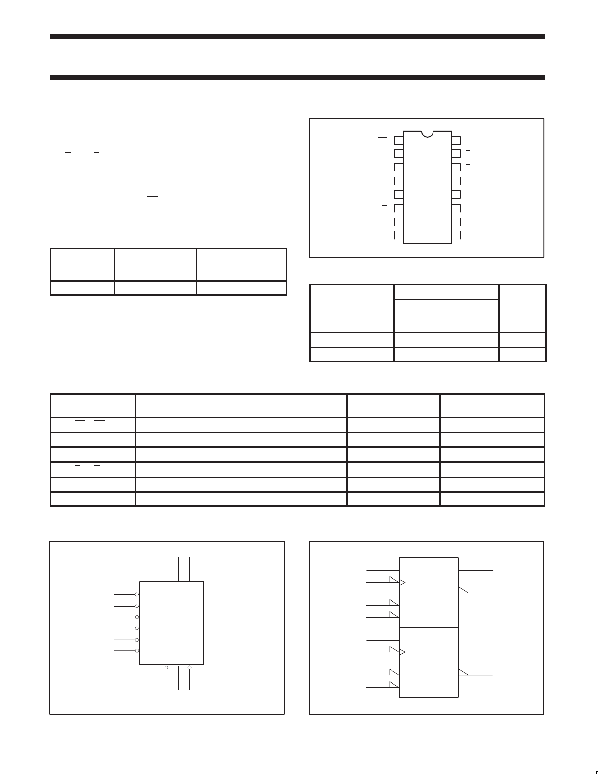
PIN CONFIGURATION
The 74ALS112A, dual negative edge-triggered JK-type flip-flop
features individual J, K, clock (CP
inputs, true (Qn) and complementary (Q
D and RD inputs, when Low, set or reset the outputs as shown
The S
in the function table regardless of the level at the other inputs.
A High level on the clock (CP
data will be accepted. The logic levels at the J and K inputs may be
allowed to change while the CP
according to the function table as long as minimum setup and hold
times are observed. Output changes are initiated by the High-to-Low
transition of the CP
n.
TYPE
74ALS112A 50MHz 3.0mA
n), set (SD), and reset (RD)
n) outputs.
n) input enables the J and K inputs and
n is High and the flip-flop will perform
TYPICAL
f
MAX
TYPICAL
SUPPLY CURRENT
(TOTAL)
1
CP0
2
K0
J0
3
S
4
D0
5
Q0
6
0
Q
1
Q
ORDERING INFORMA TION
ORDER CODE
16
15
14
13
12
11
107
98GND Q1
V
R
R
CP
K1
J1
SD1
CC
D0
D1
1
DESCRIPTION COMMERCIAL RANGE
V
= 5V ±10%,
CC
T
= 0°C to +70°C
amb
16-pin plastic DIP 74ALS1 12AN SOT38-4
16-pin plastic SO 74ALS1 12AD SOT109-1
INPUT AND OUTPUT LOADING AND FAN-OUT TABLE
PINS DESCRIPTION
74ALS (U.L.)
HIGH/LOW
CP0, CP1 Clock Pulse input (active falling edge) 1.0/1.0 20µA/0.1mA
J0, J1 J inputs 1.0/2.0 20µA/0.2mA
K0, K1 K inputs 1.0/2.0 20µA/0.2mA
SD0, SD1 Set inputs (active-Low) 1.0/2.0 20µA/0.2mA
RD0, RD1 Reset inputs (active-Low) 1.0/2.0 20µA/0.2mA
Q0, Q1, Q0, Q1 Data outputs 20/80 0.4mA/8mA
NOTE: One (1.0) ALS unit load is defined as: 20µA in the High state and 0.1mA in the Low state.
LOAD VALUE
HIGH/LOW
SF00103
DRAWING
NUMBER
LOGIC SYMBOL
212
311
J1 K0
CP0
SD0
RD0
CP1
SD1
RD1
Q0 Q0 Q1 Q1
56 97
VCC = Pin 16
GND = Pin 8
1
4
15
13
10
14
1996 Jun 27 853-1846 16995
K1J0
SF00104
IEC/IEEE SYMBOL
2
3
1
2
15
4
11
13
12
14
10
1J
C1
1K
R
S
2J
C2
2K
R
S
5
6
9
7
SF00105
Philips Semiconductors Product specification
OPERATING MODE
74ALS112ADual J-K negative edge-triggered flip-flop
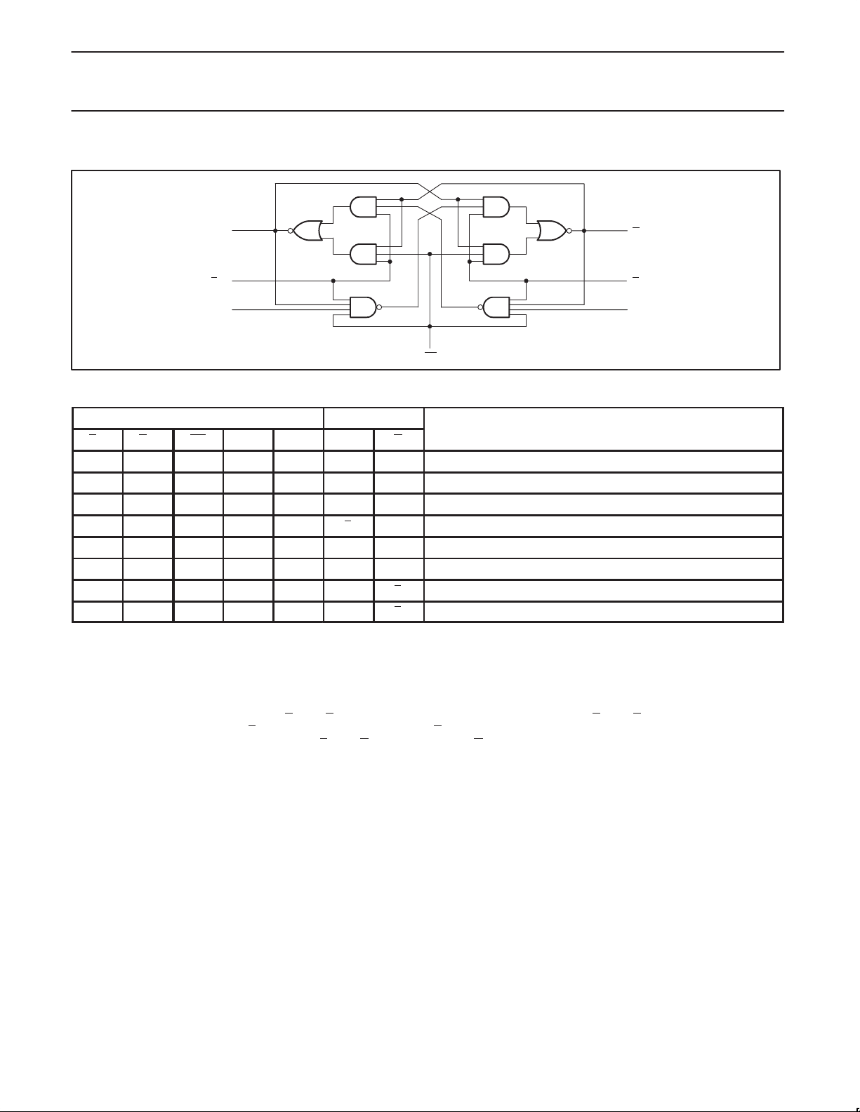
LOGIC DIAGRAM
5, 9
Qn
4, 10
S
Dn
2, 12
Kn
VCC = Pin 16
GND = Pin 8
CP
1, 13
n
FUNCTION TABLE
INPUTS OUTPUTS
SD RD CP J K Q Q
L H X X X H L Asynchronous Set
H L X X X L H Asynchronous Reset
L L X X X H* H* Undetermined *
H H ↓ h h q q T oggle
H H ↓ h l H L Load “1” (Set)
H H ↓ l h L H Load “0” (Reset)
H H ↓ l l q q Hold “no change”
H H H X X q q Hold “no change”
H = High voltage level
h = High state must be present one setup time prior to High-to-Low clock transition
L = Low voltage level
l = Low state must be present one setup time prior to High-to-Low clock transition
q = Lower case indicate the state of the referenced output prior to the High-to-Low clock transition
X = Don’t care
↓ = High-to-Low clock transition
* = Both outputs will be High while both S
Asynchronous inputs: Low input to S
Simultaneous Low on both S
D and RD are Low, but the output states are unpredictable if SD and RD go High simultaneously
D sets Q to High level, Low input to RD sets Q to Low level. Set and reset are independent of clock.
D and RD makes both Q and Q High.
6, 7
15, 14
3, 11
n
Q
R
Dn
Jn
SF00106
1996 Jun 27
3
 Loading...