

Philips 74AHCT374PW, 74AHCT374D, 74AHC374PW, 74AHC374D Datasheet

INTEGRATED CIRCUITS
DATA SH EET
74AHC374; 74AHCT374
Octal D-type flip-flop; positive
edge-trigger; 3-state
Product specification
Supersedes data of 1998 Dec 11
File under Integrated Circuits, IC06
1999 Sep 28
Philips Semiconductors Product specification
Octal D-type flip-flop; positive edge-trigger; 3-state
FEATURES
• ESD protection:
HBM EIA/JESD22-A114-A
exceeds 2000 V
MM EIA/JESD22-A115-A
exceeds 200 V
CDM EIA/JESD22-C101
exceeds 1000 V
• Balanced propagation delays
• All inputs have Schmitt-trigger
actions
• Inputsacceptsvoltageshigherthan
V
CC
• Common 3-state output enable
input
• ICC category: MSI
• For AHC only:
operates with CMOS input levels
• For AHCT only:
operates with TTL input levels
• Specified from
−40 to +85 and +125 °C.
DESCRIPTION
The 74AHC/AHCT374 are high-speed Si-gate CMOS devices and are pin
compatible with low power Schottky TTL (LSTTL). They are specified in
compliance with JEDEC standard No. 7A.
The 74AHC/AHCT374 are octal D-type flip-flops featuring separate D-type
inputs for each flip-flop and 3-state outputs for bus oriented applications.
A clock (CP) and an output enable (OE) input are common to all flip-flops.
The 8 flip-flops will store the state of their individual D-inputs that meet the
set-up and hold times requirements on the LOW-to-HIGH CP transition.
When OE is LOW the contents of the 8 flip-flops are available at the outputs.
When OE isHIGH, theoutputs go to the high-impedance OFF-state. Operation
of the OE input does not affect the state of the flip-flops.
The ‘374’ is functionally identical to the ‘534’, but has non-inverting outputs.
74AHC374;
74AHCT374
QUICK REFERENCE DATA
GND = 0 V; T
=25°C; tr=tf≤3.0 ns.
amb
SYMBOL PARAMETER CONDITIONS
t
PHL/tPLH
f
max
C
I
C
O
C
PD
propagation delay;
CP to Q
n
maximum clock frequency CL= 15 pF; VCC=5V 50 − MHz
input capacitance VI=VCCor GND 3.0 3.0 pF
output capacitance 4.0 4.0 pF
power dissipation
capacitance
CL= 15 pF; VCC= 5 V 3.5 5.0 ns
CL= 50 pF; f = 1 MHz;
notes 1 and 2
Notes
1. C
is used to determine the dynamic power dissipation (PDin µW).
PD
PD=CPD× V
2
× fi+ ∑ (CL× V
CC
2
× fo) where:
CC
fi= input frequency in MHz;
fo= output frequency in MHz;
∑ (CL× V
2
× fo) = sum of outputs;
CC
CL= output load capacitance in pF;
VCC= supply voltage in Volts.
2. The condition is VI= GND to VCC.
TYPICAL
UNIT
AHC AHCT
10 12 pF
1999 Sep 28 2
Philips Semiconductors Product specification
Octal D-type flip-flop; positive edge-trigger; 3-state
74AHC374;
74AHCT374
FUNCTION TABLE
See note 1.
OPERATING MODES
INPUTS
OE CP D
n
INTERNAL
FLIP-FLOPS
Load and read register L ↑ ILL
L↑hHH
Load register and
disable outputs
H ↑ lLZ
H↑hHZ
Note
1. H = HIGH voltage level;
h = HIGH voltage level one set-up time prior to the LOW-to-HIGH CP transition;
L = LOW voltage level;
I = LOW voltage level one set-up time prior to the LOW-to-HIGH CP transition;
X = don’t care;
Z = high-impedance OFF-state;
↑ = LOW-to-HIGH CP transition.
OUTPUTS
Q0to Q
7
ORDERING INFORMATION
OUTSIDE NORTH
AMERICA
NORTH AMERICA
PINS PACKAGE MATERIAL CODE
PACKAGES
74AHC374D 74AHC374D 20 SO plastic SOT163-1
74AHC374PW 74AHC374PW DH 20 TSSOP plastic SOT360-1
74AHCT374D 74AHCT374D 20 SO plastic SOT163-1
74AHCT374PW 7AHCT374PW DH 20 TSSOP plastic SOT360-1
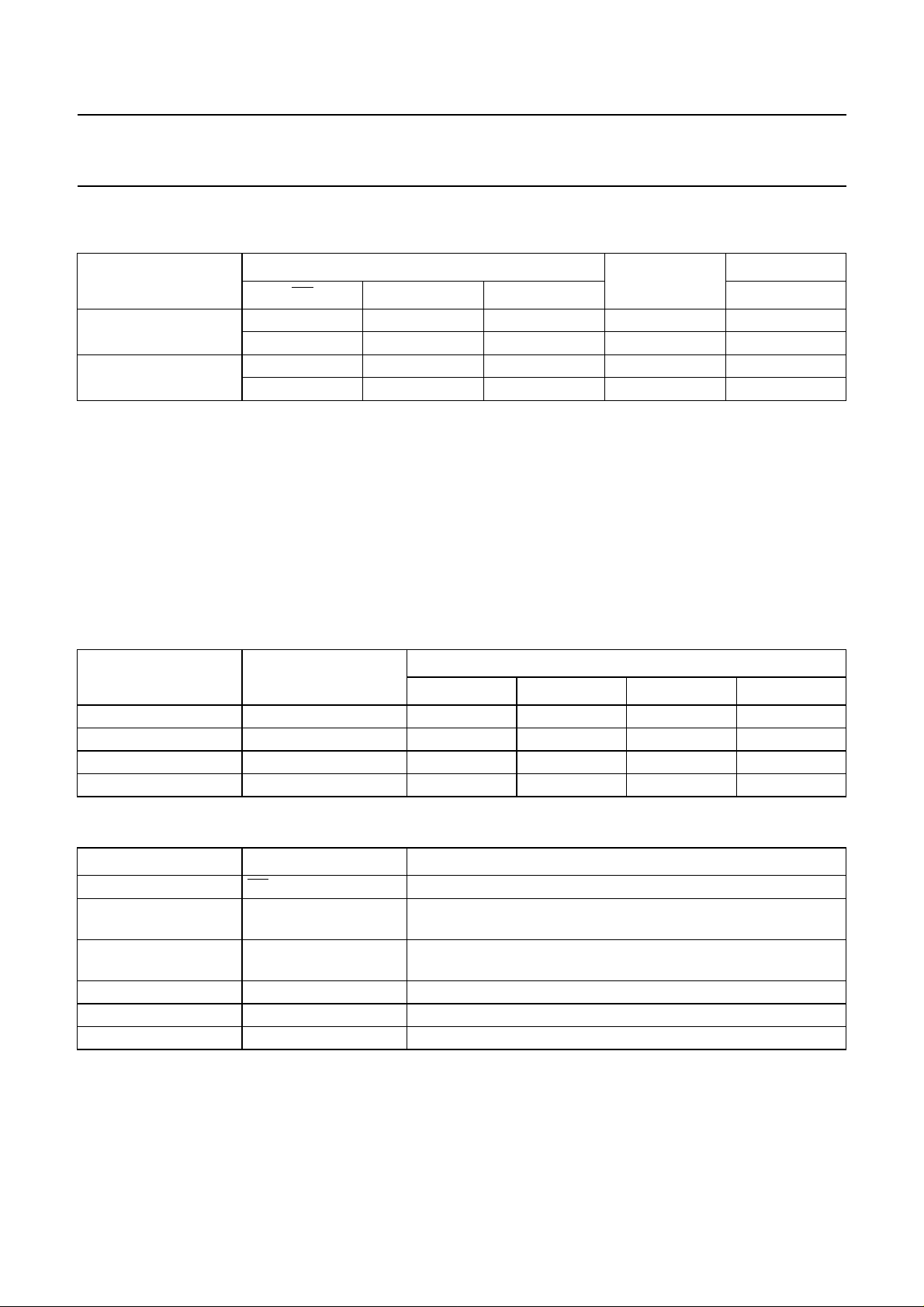
PINNING
PIN SYMBOL DESCRIPTION
1
2, 5, 6, 9, 12, 15,
OE 3-state output enable input (active LOW)
to Q
Q
0
7
3-state flip-flop outputs
16 and 19
3, 4, 7, 8, 13, 14,
D
0
to D
7
data inputs
17 and 18
10 GND ground (0 V)
11 CP clock input (LOW-to-HIGH, edge triggered)
20 V
CC
DC supply voltage
1999 Sep 28 3
Philips Semiconductors Product specification
Octal D-type flip-flop; positive edge-trigger; 3-state
handbook, halfpage
OE
Q
D
D
Q
Q
D
D
Q
GND
1
2
0
3
0
4
1
5
1
2
2
3
3
374
6
7
8
9
10
MNA194
V
20
CC
Q
19
7
D
18
7
D
17
6
Q
16
6
Q
15
5
D
14
5
D
13
4
Q
12
4
CP
11
handbook, halfpage
74AHC374;
74AHCT374
11
3
4
7
8
13
14
17
18
CP
D
0
D
1
D
2
D
3
D
4
D
5
D
6
D
7
OE
1
Q
Q
Q
Q
Q
Q
Q
Q
0
1
2
3
4
5
6
7
MNA195
2
5
6
9
12
15
16
19
handbook, halfpage
Fig.1 Pin configuration.
1
EN
11
C1
3
1D
4
7
8
13
14
17
18
MNA196
2
5
6
9
12
15
16
19
handbook, halfpage
3
4
7
8
13
14
17
18
11
1
Fig.2 Logic symbol.
D
0
D
1
D
2
D
D
D
D
D
CP
OE
FF1
3
to
4
FF8
5
6
7
3-STATE
OUTPUTS
Q
0
Q
1
Q
2
Q
3
Q
4
Q
5
Q
6
Q
7
MNA197
2
5
6
9
12
15
16
19
Fig.3 IEC logic symbol.
1999 Sep 28 4
Fig.4 Functional diagram.
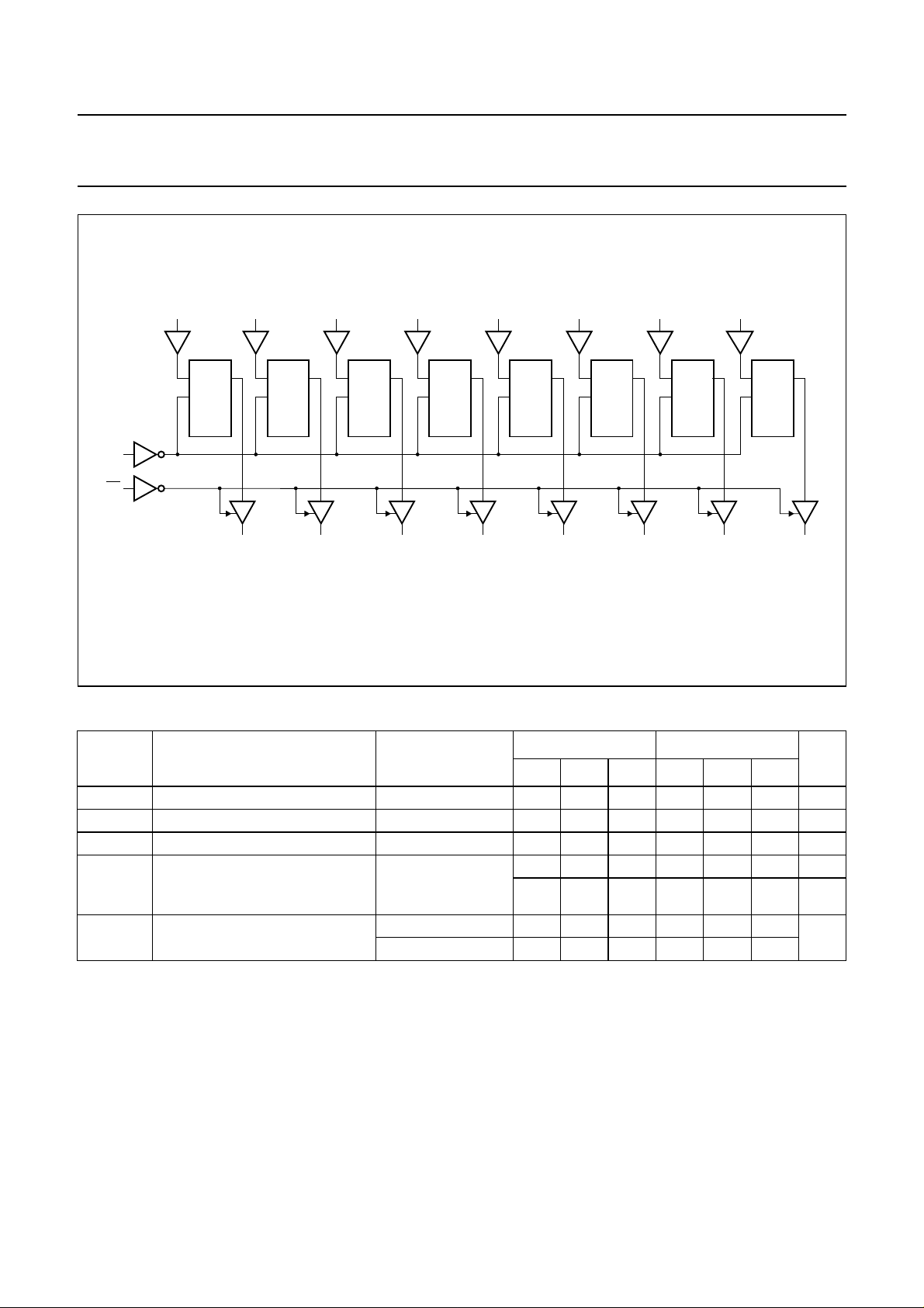
Philips Semiconductors Product specification
Octal D-type flip-flop; positive edge-trigger; 3-state
D
4
Q
D
Q
CP
FF5
Q
3
Q
4
CP
OE
D
0
D
CP
FF1
D
1
Q
D
CP
FF2
Q
0
D
2
Q
D
CP
FF3
Q
1
D
3
Q
D
CP
FF4
Q
2
74AHC374;
74AHCT374
D
5
D
CP
FF6
D
6
Q
D
CP
FF7
Q
5
D
7
Q
D
Q
CP
FF8
Q
6
Q
MNA198
7
Fig.5 Logic diagram.
RECOMMENDED OPERATING CONDITIONS
74AHC 74AHCT
SYMBOL PARAMETER CONDITIONS
MIN. TYP. MAX. MIN. TYP. MAX.
V
CC
V
I
V
O
T
amb
DC supply voltage 2.0 5.0 5.5 4.5 5.0 5.5 V
input voltage 0 − 5.5 0 − 5.5 V
output voltage 0 − V
operating ambient temperature
range
see DC and AC
characteristics per
−40 +25 +85 −40 +25 +85 °C
−40 +25 +125 −40 +25 +125 °C
0 − V
CC
CC
device
t
(∆t/∆f) input rise and fall rates VCC= 3.3 V ±0.3 V −−100 −−−ns/V
r,tf
V
=5V±0.5 V −−20 −−20
CC
UNIT
V
1999 Sep 28 5
Philips Semiconductors Product specification
Octal D-type flip-flop; positive edge-trigger; 3-state
74AHC374;
74AHCT374
LIMITING VALUES
In accordance with the Absolute Maximum Rating System (IEC 134); voltages are referenced to GND (ground= 0 V).
SYMBOL PARAMETER CONDITIONS MIN. MAX. UNIT
V
CC
V
I
I
IK
I
OK
I
O
I
CC
T
stg
P
D
Notes
1. The input and output voltage ratings may be exceeded if the input and output current ratings are observed.
2. For SO packages: above 70 °C the value of P
For TSSOP packages: above 60 °C the value of PDderates linearly with 5.5 mW/K.
DC supply voltage −0.5 +7.0 V
input voltage range −0.5 +7.0 V
DC input diode current VI< −0.5 V; note 1 −−20 mA
DC output diode current VO< −0.5 Vor VO>VCC+ 0.5 V; note 1 −±20 mA
DC output source or sink current −0.5V<VO<VCC+ 0.5 V −±25 mA
DC VCC or GND current −±75 mA
storage temperature range −65 +150 °C
power dissipation per package for temperature range: −40 to +125 °C; note 2 − 500 mW
derates linearly with 8 mW/K.
D
1999 Sep 28 6
 Loading...