

Philips 74AHCT1G32GW, 74AHC1G32GW Datasheet

INTEGRATED CIRCUITS
DATA SH EET
74AHC1G32; 74AHCT1G32
2-input OR gate
Product specification
Supersedes data of 1998 Nov 25
File under Integrated Circuits, IC06
1999 Jan 27
Philips Semiconductors Product specification
2-input OR gate 74AHC1G32; 74AHCT1G32
FEATURES
• Symmetrical output impedance
• High noise immunity
• ESD protection:
HBM EIA/JESD22-A114-A
exceeds 2000 V
MM EIA/JESD22-A115-A exceeds
200 V
• Low power dissipation
• Balanced propagation delays
• Very small 5-pin package
• Output capability: standard.
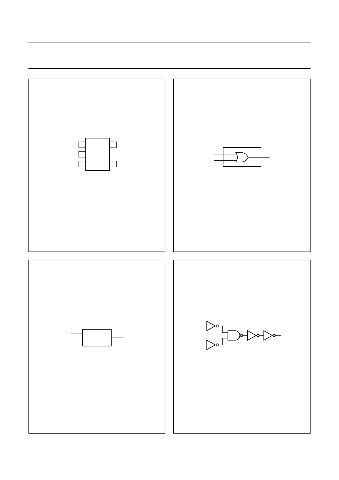
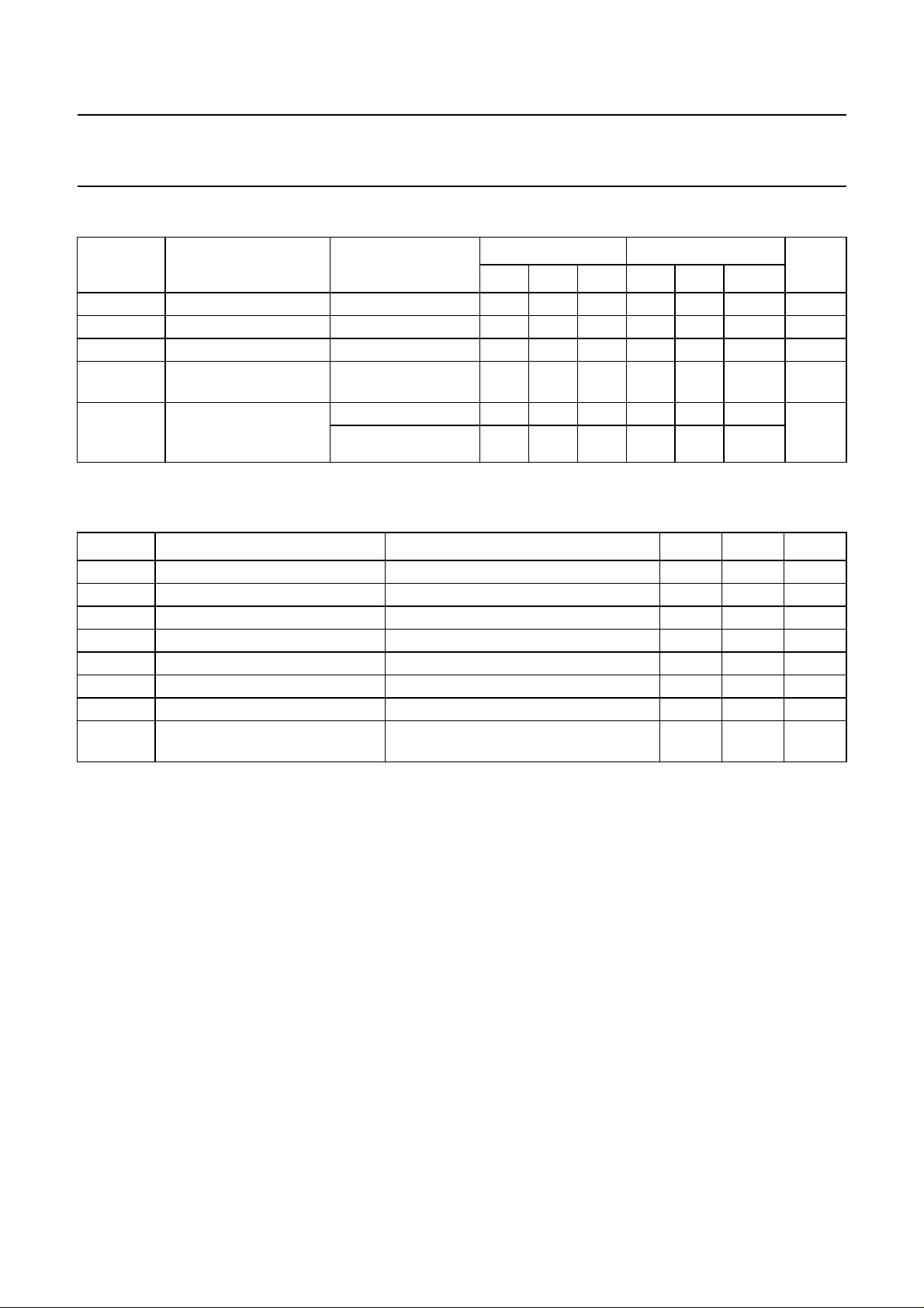
DESCRIPTION
The 74AHC1G/AHCT1G32 is a
high-speed Si-gate CMOS device.
The 74AHC1G/AHCT1G32 provides
the 2-input OR function.
FUNCTION TABLE
See note 1.
QUICK REFERENCE DATA
GND = 0 V; T
=25°C; tr=tf≤3.0 ns.
amb
SYMBOL PARAMETER CONDITIONS
t
PHL/tPLH
C
I
C
PD
propagation delay
inA, inB to outY
input capacitance 1.5 1.5 pF
power dissipation
capacitance
CL=15pF
VCC=5V
notes 1 and 2;
CL= 50 pF;
f=1MHz
Notes
1. C
is used to determine the dynamic power dissipation (PDin µW).
PD
PD=CPD× V
2
× fi+(CL×V
CC
2
× fo) where.
CC
fi= input frequency in MHz;
fo= output frequency in MHz;
CL= output load capacitance in pF;
VCC= supply voltage in V.
2. The condition is VI= GND to VCC.
PINNING
TYPICAL
UNIT
AHC1G AHCT1G
3.2 3.3 ns
16 17 pF
INPUTS OUTPUT
inA inB outY
LL L
LH H
HL H
HH H
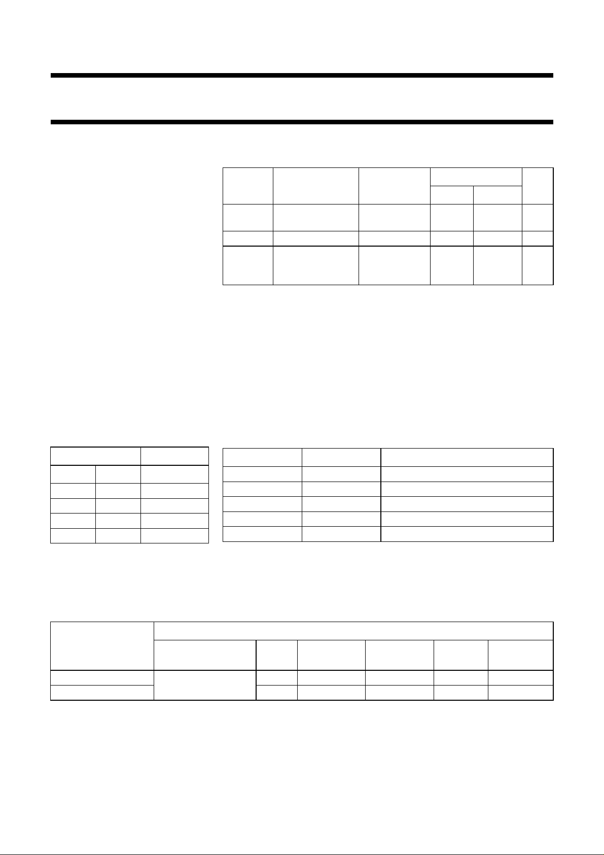
PIN SYMBOL DESCRIPTION
1 inB data input B
2 inA data input A
3 GND ground (0 V)
4 outY data output
5V
CC
DC supply voltage
Note
1. H = HIGH voltage level.
L = LOW voltage level.
ORDERING INFORMATION
PACKAGES
TYPE NUMBER
74AHC1G32GW
74AHCT1G32GW 5 SC-88A plastic SOT353 CG
TEMPERATURE
RANGE
−40 to +85 °C
PINS PACKAGE MATERIAL CODE MARKING
5 SC-88A plastic SOT353 AG
1999 Jan 27 2
Philips Semiconductors Product specification
2-input OR gate 74AHC1G32; 74AHCT1G32
handbook, halfpage
inB
inA
GND
1
2
32
3
MNA163
V
5
outY
4
Fig.1 Pin configuration.
CC
handbook, halfpage
1
inB
2
inA
outY
MNA164
Fig.2 Logic symbol.
4
handbook, halfpage
1
2
≥1
4
MNA165
Fig.3 IEC logic symbol.
1999 Jan 27 3
handbook, halfpage
inB
inA
outY
MNA166
Fig.4 Logic diagram.
Philips Semiconductors Product specification
2-input OR gate 74AHC1G32; 74AHCT1G32
RECOMMENDED OPERATING CONDITIONS
SYMBOL PARAMETER CONDITIONS
UNIT
MIN. TYP. MAX. MIN. TYP. MAX.
74AHC1G 74AHCT1G
V
CC
V
I
V
O
T
amb
DC supply voltage 2.0 5.0 5.5 4.5 5.0 5.5 V
input voltage 0 − 5.5 0 − 5.5 V
output voltage 0 − V
operating ambient
−40 +25 +85 −40 +25 +85 °C
0 − V
CC
CC
V
temperature range
t
(∆t/∆f) input rise and fall times
r,tf
except for
Schmitt-trigger inputs
VCC= 3.3 V ±0.3 V −−100 −−− ns/V
V
=5V±0.5 V −−20 −−20
CC
LIMITING VALUES
In accordance with the Absolute Maximum Rating System (IEC 134); voltages are referenced to GND (ground = 0 V).
SYMBOL PARAMETER CONDITIONS MIN. MAX. UNIT
V
CC
V
I
I
IK
I
OK
I
O
I
CC
T
stg
P
D
DC supply voltage −0.5 +7.0 V
input voltage range −0.5 +7.0 V
DC input diode current VI< −0.5 −−20 mA
DC output diode current VO< −0.5 or VO>VCC+ 0.5 V; note 1 −±20 mA
DC output source or sink current −0.5V<VO<VCC+ 0.5 V −±25 mA
DC VCC or GND current −±75 mA
storage temperature range −65 +150 °C
power dissipation per package temperature range: −40 to +85 °C;
− 200 mW
note 2
Notes
1. The input and output voltage ratings may be exceeded if the input and output current ratings are observed.
2. Above +55 °C the value of P
derates linearly with 2.5 mW/K.
D
1999 Jan 27 4
 Loading...