

Philips 74AHC126PW, 74AHC126D, 74AHCT126PW, 74AHCT126D Datasheet

INTEGRATED CIRCUITS
DATA SH EET
74AHC126; 74AHCT126
Quad buffer/line driver; 3-state
Product specification
Supersedes data of 1999 Jan 12
File under Integrated Circuits, IC06
1999 Sep 29
Philips Semiconductors Product specification
Quad buffer/line driver; 3-state 74AHC126; 74AHCT126
FEATURES
• ESD protection:
HBM EIA/JESD22-A114-A
exceeds 2000 V
MM EIA/JESD22-A115-A
exceeds 200 V
CDM EIA/JESD22-C101
exceeds 1000 V
• Balanced propagation delays
• All inputs have Schmitt-trigger
actions
• Inputsacceptsvoltageshigherthan
V
CC
• For AHC only:
operates with CMOS input levels
• For AHCT only:
operates with TTL input levels
• Specified from
−40 to +85 and +125 °C.
DESCRIPTION
The 74AHC/AHCT126 are
high-speed Si-gate CMOS devices
and are pin compatible with low
power Schottky TTL (LSTTL). They
are specified in compliance with
JEDEC standard No. 7A.
The 74AHC/AHCT126 are four
non-inverting buffer/line drivers with
3-state outputs. The 3-state outputs
(nY) are controlled by the output
enable input (nOE) A LOW at nOE
causes the outputs to assume a
HIGH-impedance OFF state.
The ‘126’ is identical to the ‘125’ but
has active HIGH enable inputs.
FUNCTION TABLE
See note 1.
INPUTS OUTPUT
nOE nA nY
HLL
HHH
LXZ
Note
1. H = HIGH voltage level;
L = LOW voltage level;
X = don’t care;
Z = high-impedance OFF state.
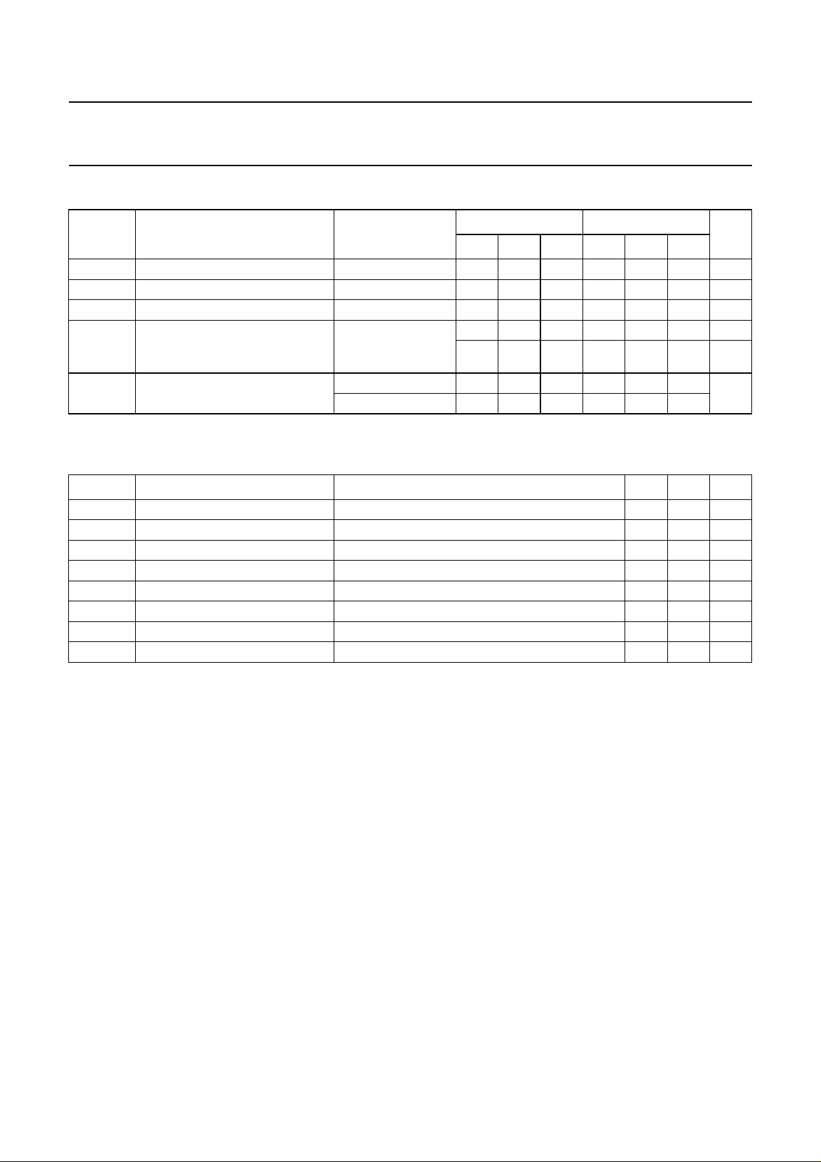
QUICK REFERENCE DATA
GND = 0 V; T
=25°C; tr=tf≤3.0 ns.
amb
SYMBOL PARAMETER CONDITIONS
t
PHL/tPLH
C
I
C
O
C
PD
propagation delay
nA to nY
input capacitance VI=VCCor GND 3.0 3.0 pF
output capacitance 4.0 4.0 pF
power dissipation
capacitance
CL=15pF;
VCC=5V
CL=50pF;
f = 1 MHz;
notes 1 and 2
Notes
1. C
is used to determine the dynamic power dissipation (PDin µW).
PD
PD=CPD× V
2
× fi+ ∑ (CL× V
CC
2
× fo) where:
CC
fi= input frequency in MHz;
fo= output frequency in MHz;
∑ (CL× V
2
× fo) = sum of outputs;
CC
CL= output load capacitance in pF;
VCC= supply voltage in Volts.
2. The condition is VI= GND to VCC.
TYPICAL
UNIT
AHC AHCT
3.3 3.0 ns
10 12 pF
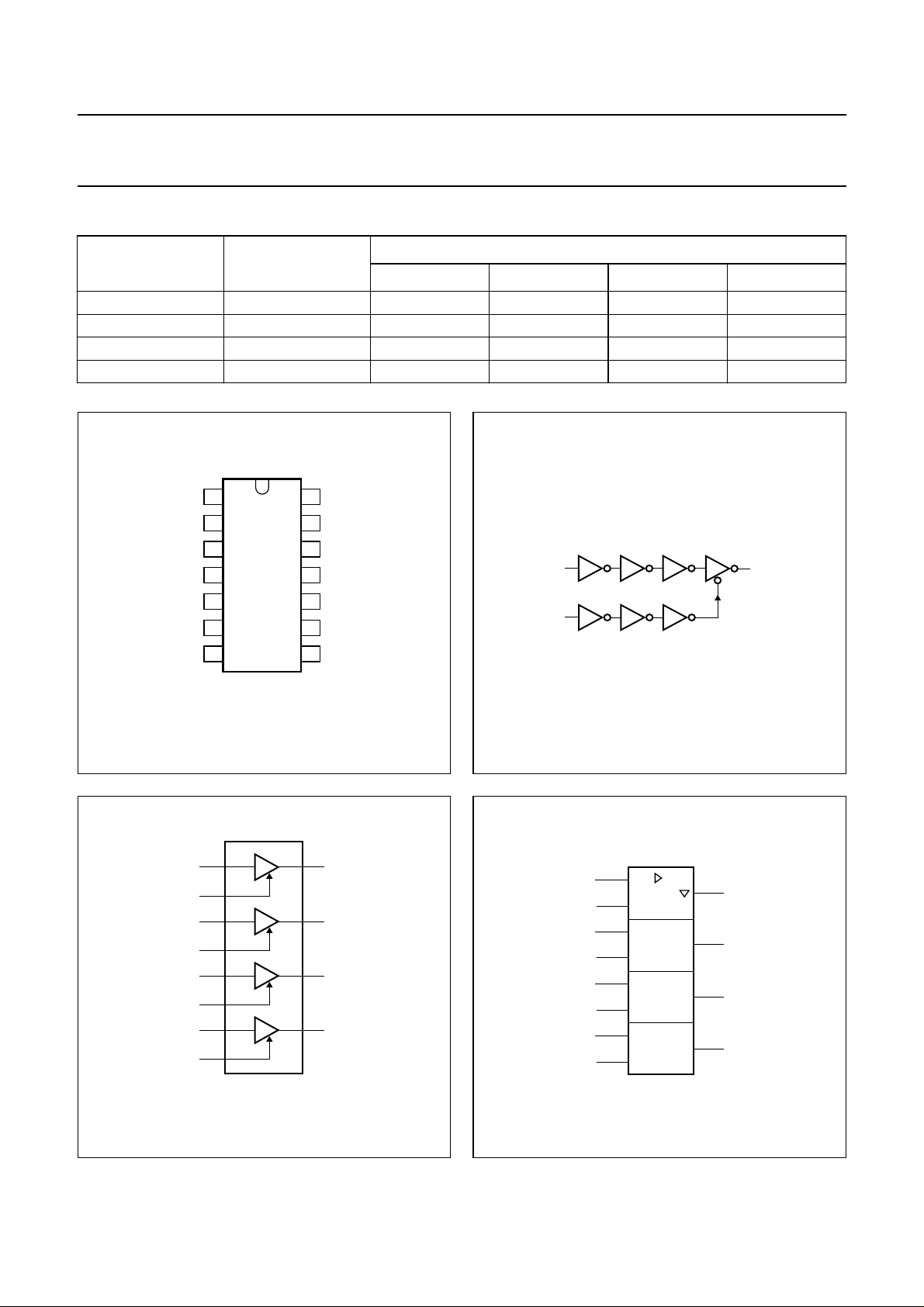
PINNING
PIN SYMBOL DESCRIPTION
1, 4, 10 and 13 1OE to 4OE output enable inputs (active HIGH)
2, 5, 9 and 12 1A to 4A data inputs
3, 6, 8 and 11 1Y to 4Y data outputs
7 GND ground (0 V)
14 V
1999 Sep 29 2
CC
DC supply voltage
Philips Semiconductors Product specification
Quad buffer/line driver; 3-state 74AHC126; 74AHCT126
ORDERING INFORMATION
OUTSIDE NORTH
AMERICA
NORTH AMERICA
PINS PACKAGE MATERIAL CODE
PACKAGES
74AHC126D 74AHC126D 14 SO plastic SOT108-1
74AHC126PW 74AHC126PW DH 14 TSSOP plastic SOT402-1
74AHCT126D 74AHCT126D 14 SO plastic SOT108-1
74AHCT126PW 7AHCT126PW DH 14 TSSOP plastic SOT402-1
1OE
1A
1Y
2OE
2A
2Y
GND
1
2
3
4
126
5
6
7
MNA233
V
14
CC
13
4OE
12
4A
11
4Y
10
3OE
9
3A
8
3Y
handbook, halfpage
nOE
nA
nY
MNA234
handbook, halfpage
Fig.1 Pin configuration.
2
1
5
4
9
10
12
13
1A 1Y
1OE
2A 2Y
2OE
3A 3Y
3OE
4A 4Y
4OE
MNA235
3
6
8
11
Fig.3 Functional diagram.
handbook, halfpage
Fig.2 Logic diagram.
2
1
5
4
9
10
12
13
EN1
1
MNA236
3
6
8
11
Fig.4 IEC logic symbol.
1999 Sep 29 3
Philips Semiconductors Product specification
Quad buffer/line driver; 3-state 74AHC126; 74AHCT126
RECOMMENDED OPERATING CONDITIONS
SYMBOL PARAMETER CONDITIONS
UNIT
MIN. TYP. MAX. MIN. TYP. MAX.
74AHC 74AHCT
V
CC
V
I
V
O
T
amb
DC supply voltage 2.0 5.0 5.5 4.5 5.0 5.5 V
input voltage 0 − 5.5 0 − 5.5 V
output voltage 0 − V
operating ambient temperature
range
see DC and AC
characteristics per
−40 +25 +85 −40 +25 +85 °C
−40 +25 +125 −40 +25 +125 °C
0 − V
CC
CC
V
device
t
(∆t/∆f) input rise and fall rates VCC= 3.3 V ±0.3 V −−100 −−−ns/V
r,tf
=5V±0.5 V −−20 −−20
V
CC
LIMITING VALUES
In accordance with the Absolute Maximum Rating System (IEC 134); voltages are referenced to GND (ground= 0 V).
SYMBOL PARAMETER CONDITIONS MIN. MAX. UNIT
V
CC
V
I
I
IK
I
OK
I
O
I
CC
T
stg
P
D
DC supply voltage −0.5 +7.0 V
input voltage range −0.5 +7.0 V
DC input diode current VI< −0.5 V; note 1 −−20 mA
DC output diode current VO< −0.5 Vor VO>VCC+ 0.5 V; note 1 −±20 mA
DC output source or sink current −0.5V<VO<VCC+ 0.5 V −±25 mA
DC VCC or GND current −±75 mA
storage temperature range −65 +150 °C
power dissipation per package for temperature range: −40 to +125 °C; note 2 − 500 mW
Notes
1. The input and output voltage ratings may be exceeded if the input and output current ratings are observed.
2. For SO packages: above 70 °C the value of P
derates linearly with 8 mW/K.
D
For TSSOP packages: above 60 °C the value of PDderates linearly with 5.5 mW/K.
1999 Sep 29 4
Philips Semiconductors Product specification
Quad buffer/line driver; 3-state 74AHC126; 74AHCT126
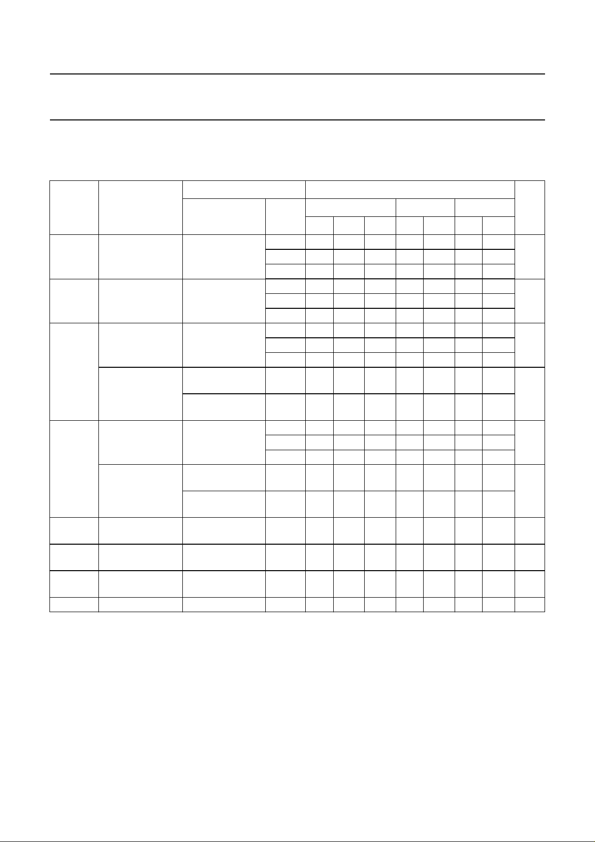
DC CHARACTERISTICS
74AHC family
Over recommended operating conditions; voltages are referenced to GND (ground=0V).
SYMBOL PARAMETER
V
IH
HIGH-level input
voltage
V
IL
LOW-level input
voltage
V
OH
HIGH-level output
voltage; all
outputs
HIGH-level output
voltage
V
OL
LOW-level output
voltage; all
outputs
LOW-level output
voltage
I
I
input leakage
current
I
OZ
3-state output
OFF current
I
CC
quiescent supply
current
C
I
input capacitance −−310−10 − 10 pF
TEST CONDITIONS T
25 −40 to +85 −40 to +125
amb
(°C)
UNIT
OTHER VCC(V)
MIN. TYP. MAX. MIN. MAX. MIN. MAX.
2.0 1.5 −−1.5 − 1.5 − V
3.0 2.1 −−2.1 − 2.1 −
5.5 3.85 −−3.85 − 3.85 −
2.0 −− 0.5 − 0.5 − 0.5 V
3.0 −− 0.9 − 0.9 − 0.9
5.5 −− 1.65 − 1.65 − 1.65
VI=VIHor VIL;
IO= −50 µA
2.0 1.9 2.0 − 1.9 − 1.9 − V
3.0 2.9 3.0 − 2.9 − 2.9 −
4.5 4.4 4.5 − 4.4 − 4.4 −
V
I=VIH
or VIL;
3.0 2.58 −−2.48 − 2.40 − V
IO= −4.0 mA
V
I=VIH
or VIL;
4.5 3.94 −−3.8 − 3.70 −
IO= −8.0 mA
VI=VIHor VIL;
IO=50µA
2.0 − 0 0.1 − 0.1 − 0.1 V
3.0 − 0 0.1 − 0.1 − 0.1
4.5 − 0 0.1 − 0.1 − 0.1
V
I=VIH
or VIL;
3.0 −− 0.36 − 0.44 − 0.55 V
IO=4mA
V
I=VIH
or VIL;
4.5 −− 0.36 − 0.44 − 0.55
IO=8mA
VI=VCCor GND 5.5 −− 0.1 − 1.0 − 2.0 µA
VI=VIHor VIL;
5.5 −− ±0.25 −±2.5 −±10.0 µA
VO=VCCor GND
VI=VCCor GND;
5.5 −− 2.0 − 20 − 40 µA
IO=0
1999 Sep 29 5
 Loading...