

Philips 74AHCT123A, 74AHC123A Datasheet

INTEGRATED CIRCUITS
DATA SH EET
74AHC123A; 74AHCT123A
Dual retriggerable monostable
multivibrator with reset
Product specification
File under Integrated Circuits, IC06
2000 Mar 15

Philips Semiconductors Product specification
Dual retriggerable monostable multivibrator
with reset
FEATURES
• ESD protection:
HBM EIA/JESD22-A114-A exceeds 2000 V
MM EIA/JESD22-A115-A exceeds 200 V
CDM EIA/JESD22-C101 exceeds 1000 V
• All inputs have Schmitt-trigger actions
• Inputs accept voltages higher than V
CC
• For AHC only: operates with CMOS input levels
• For AHCT only: operates with TTL input levels
• Specified from −40 to +85 °C and −40 to +125 °C
• DC triggered from active HIGH or active LOW inputs
• Retriggerable for very long pulses up to 100% duty
factor
• Direct reset terminates output pulse
• Output capability: standard (except for nR
EXT/CEXT
).
DESCRIPTION
The 74AHC/AHCT123A are high-speed Si-gate CMOS
devices and are pin compatible with Low power Schottky
TTL (LSTTL). They are specified in compliance with
JEDEC standard no.7A.
Once triggered, the basic output pulse width may be
extendedbyretriggeringthegatedactiveLOW-goingedge
input (nA) or the active HIGH-going edge input (nB).
By repeating this process, the output pulse period
(nQ = HIGH, nQ = LOW) can be made as long as desired.
Alternativelyan output delay can beterminatedat any time
by a LOW-going edgeon input nRD, which also inhibitsthe
triggering.
An internal connection from nRDto the input gate makes it
possible to trigger the circuit by a positive-going signal at
input nRD as shown in the function table. Figs 8 and 9
illustrate pulse control by retriggering and early reset. The
basic output pulse width is essentially determined by the
value of the external timing components R
When C
definedas: tW=R
R
EXT
in pF. Schmitt-trigger action at all inputs makes the circuit
highly tolerant to slower input rise and fall times. The ‘123’
is identical to the ‘423’ but can be triggered via the reset
input.
74AHC123A;
74AHCT123A
≥ 10 nF, the typical output pulse width is
EXT
× C
EXT
= external resistor in kΩ; C
wheretW= pulsewidth in ns;
EXT
= external capacitor
EXT
EXT
and C
EXT
.
The74AHC/AHCT123Aaredualretriggerablemonostable
multivibrators with output pulse width control by three
methods. The basic pulse time is programmed by
selection of an external resistor (R
(C
). The external resistor and capacitor are normally
EXT
) and capacitor
EXT
connected as shown in Fig.6.
2000 Mar 15 2

Philips Semiconductors Product specification
Dual retriggerable monostable multivibrator
with reset
QUICK REFERENCE DATA
GND = 0 V; T
SYMBOL PARAMETER CONDITIONS
t
PHL/tPLH
C
I
C
O
C
PD
Notes
1. C
is used to determine the dynamic power dissipation (PDin µW).
PD
PD=CPD× V
fi= input frequency in MHz;
fo= output frequency in MHz;
∑ (CL× V
D = duty factor in %;
CL= output load capacitance in pF;
C
= timing capacitance in pF;
EXT
VCC= supply voltage in Volts.
2. The condition is VI= GND to VCC.
=25°C; tr=tf≤3.0 ns.
amb
propagation delay CL= 15 pF; VCC=5V;
R
=5kΩ; C
n
A, nB to nQ, nQ 5.1 5.0 ns
n
RDto nQ, nQ 5.6 5.2 ns
EXT
input capacitance VI=VCCor GND 5 3 pF
output capacitance 4 4 pF
power dissipation capacitance CL= 50 pF; f = 1 MHz; notes 1
and 2
2
× fi+ ∑ (CL× V
CC
2
× fo) = sum of outputs;
CC
CC
2
× fo) × C
EXT
× V
2
× fo+D×16 × VCCwhere:
CC
EXT
74AHC123A;
74AHCT123A
TYPICAL
UNIT
AHC AHCT
=0pF
57 58 pF
2000 Mar 15 3

Philips Semiconductors Product specification
Dual retriggerable monostable multivibrator
with reset
74AHC123A;
74AHCT123A
FUNCTION TABLE
See note 1.
INPUTS OUTPUTS
R
n
D
nAnB nQ nQ
LXX L H
XHX L
XXL L
HL↑
H ↓ H
↑ LH
(2)
(2)
(3) (4)
(3) (4)
(3) (4)
(2)
H
(2)
H
Notes
1 H = HIGH voltage level;
L = LOW voltage level;
X = don’t care;
↑ = LOW-to-HIGH CP transition;
↓ = HIGH-to-LOW CP transition.
2 If the monostable multivibrator was triggered before this condition was established, the pulse will be continued as
programmed.
3 One HIGH-level output pulse.
4 One LOW-level output pulse.
ORDERING INFORMATION
PACKAGES
TYPE NUMBER
TEMPERATURE
RANGE
PINS PACKAGE MATERIAL CODE
74AHC123AD −40 to +125 °C 16 SO plastic SOT109-1
74AHC123APW 16 TSSOP plastic SOT403-1
74AHCT123AD 16 SO plastic SOT109-1
74AHCT123APW 16 TSSOP plastic SOT403-1
2000 Mar 15 4
Philips Semiconductors Product specification
Dual retriggerable monostable multivibrator
with reset
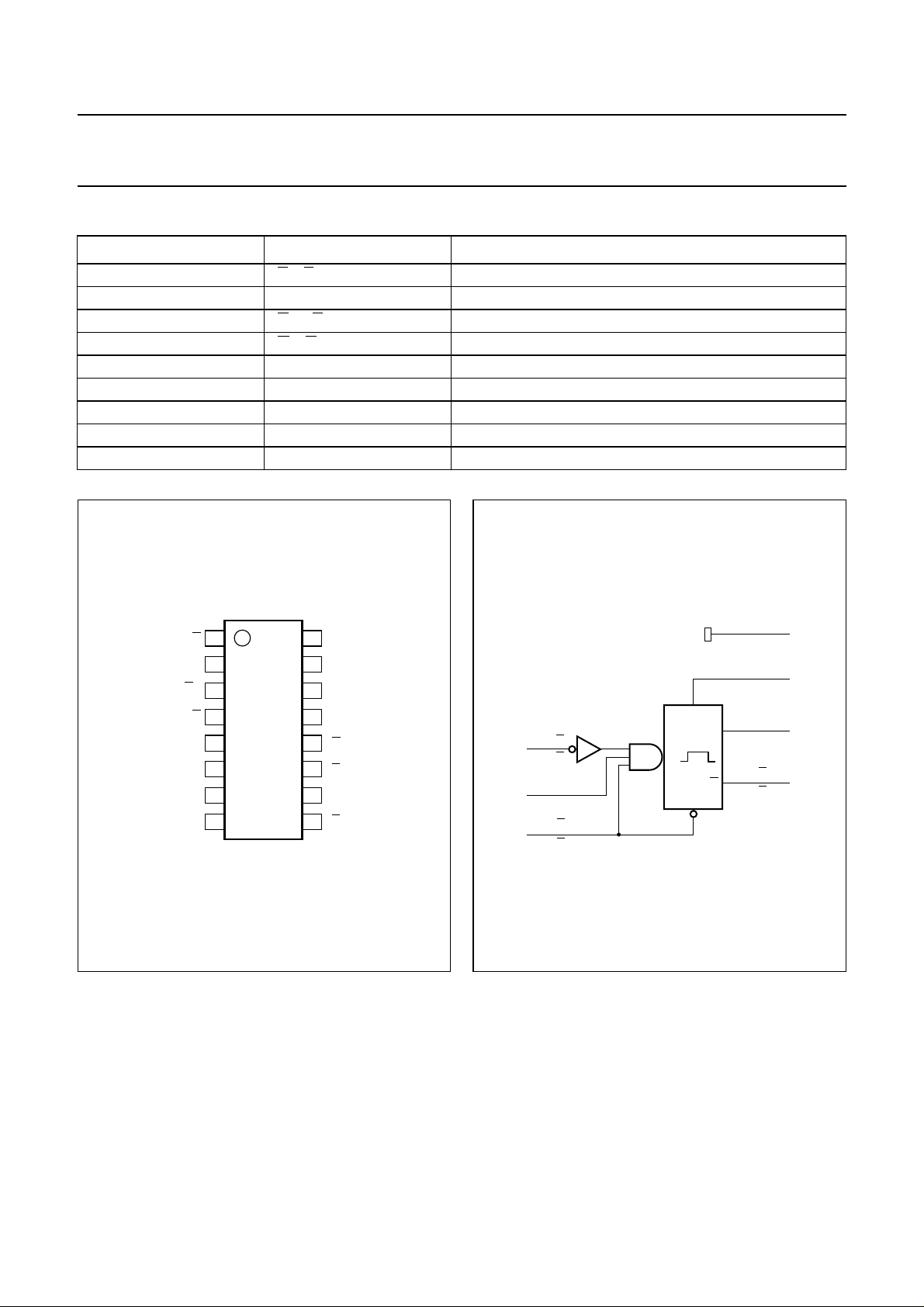
PINNING
PIN SYMBOL DESCRIPTION
1, 9 1
2, 10 1B, 2B trigger inputs (positive-edge triggered)
3, 11 1
4, 12 1
5, 13 2Q, 1Q outputs (active HIGH)
6, 14 2C
7, 15 2R
8 GND ground (0 V)
16 V
A, 2A trigger inputs (negative-edge triggered)
RD,2R
D
direct reset LOW and trigger action at positive edge
Q, 2Q outputs (active LOW)
, 1C
EXT
EXT/CEXT
CC
EXT
, 1R
EXT/CEXT
external capacitor connection
external resistor/capacitor connection
DC supply voltage
74AHC123A;
74AHCT123A
handbook, halfpage
2R
EXT/CEXT
1A
1
2
1B
1R
3
D
1Q
4
123
5
2Q
6
2C
EXT
7
GND
8
MNA514
Fig.1 Pin configuration.
16
15
14
13
12
11
10
9
V
CC
1R
EXT/CEXT
1C
EXT
1Q
2Q
2R
D
2B
2A
handbook, halfpage
11A
9
2
10 2B
3
11
2A
1B
1R
D
2R
D
Fig.2 Logic diagram.
1C
14
EXT
2C
1R
EXT/CEXT
2R
EXT/CEXT
S
Q
T
R
D
EXT
1Q
2Q 5
1QQ4
2Q 12
MNA515
6
15
7
13
2000 Mar 15 5

Philips Semiconductors Product specification
Dual retriggerable monostable multivibrator
with reset
handbook, halfpage
14
15
1
2
3
6
7
9
10
11
CX
RCX
&
R
CX
RCX
&
R
13
4
5
12
MNA516
handbook, halfpage
11A
9
2
10 2B
3
11
2A
1B
1R
2R
74AHC123A;
74AHCT123A
1C
14
EXT
2C
1R
EXT/CEXT
2R
EXT/CEXT
S
Q
T
R
D
D
D
EXT
1Q
2Q 5
1QQ4
2Q 12
MNA517
6
15
7
13
Fig.3 IEC logic symbol.
Fig.4 Functional diagram.
2000 Mar 15 6

Philips Semiconductors Product specification
Dual retriggerable monostable multivibrator
with reset
handbook, full pagewidth
R
D
CL
R
CL
V
CC
R
R
V
CC
nR
EXT/CEXT
V
CC
74AHC123A;
74AHCT123A
Q
Q
CL
MNA518
A
B
For minimum noise generation, it is recommended to ground pins 6 (2CEXT) and 14 (1CEXT) externally to pin 8 (GND).
R
CL CL
Fig.5 Logic diagram (one flip-flop).
2000 Mar 15 7

Philips Semiconductors Product specification
Dual retriggerable monostable multivibrator
with reset
handbook, halfpage
C
to nC
EXT
(pin 14 or 6)
EXT
V
to nR
EXT/CEXT
(pin 15 or 7)
CC
MNA519
R
EXT
74AHC123A;
74AHCT123A
Fig.6 Timing component connections.
RECOMMENDED OPERATING CONDITIONS
SYMBOL PARAMETER CONDITIONS
V
CC
V
I
V
O
T
amb
t
, t
r
f
R
EXT
C
EXT
DC supply voltage 2.0 5.0 5.5 4.5 5.0 5.5 V
input voltage 0 − 5.5 0 − 5.5 V
output voltage 0 − V
operating ambient
temperature
input rise and fall
time ratios
external timing
resistor
see DC and AC
characteristics per device
VCC= 3.3 ±0.3 V −−100 −−−ns/V
V
=5±0.5 V −−20 −−20 ns/V
CC
VCC=2V 5 −−5−−kΩ
V
>3V 1 −−1−−kΩ
CC
external timing
capacitor
74AHC 74AHCT
UNIT
MIN. TYP. MAX. MIN. TYP. MAX.
0 − V
CC
CC
V
−40 +25 +85 −40 +25 +85 °C
−40 +25 +125 −40 +25 +125 °C
no limits pF
2000 Mar 15 8
 Loading...