

Philips 74AHCT04D, 74AHCT04PW, 74AHC04PW, 74AHC04D Datasheet

INTEGRATED CIRCUITS
DATA SH EET
74AHC04; 74AHCT04
Hex inverter
Product specification
Supersedes data of 1999 Feb 25
File under Integrated Circuits, IC06
1999 Sep 27
Philips Semiconductors Product specification
Hex inverter 74AHC04; 74AHCT04
FEATURES
• ESD protection:
HBM EIA/JESD22-A114-A
exceeds 2000 V
MM EIA/JESD22-A115-A
exceeds 200 V
• Balanced propagation delays
• Inputsacceptsvoltageshigherthan
V
CC
• For AHC only:
operates with CMOS input levels
• For AHCT only:
operates with TTL input levels
• Specified from
−40 to +85 and +125 °C.
DESCRIPTION
The 74AHC/AHCT04 are high-speed
Si-gate CMOS devices and are pin
compatible with low power Schottky
TTL (LSTTL). They are specified in
compliance with JEDEC standard
No. 7A.
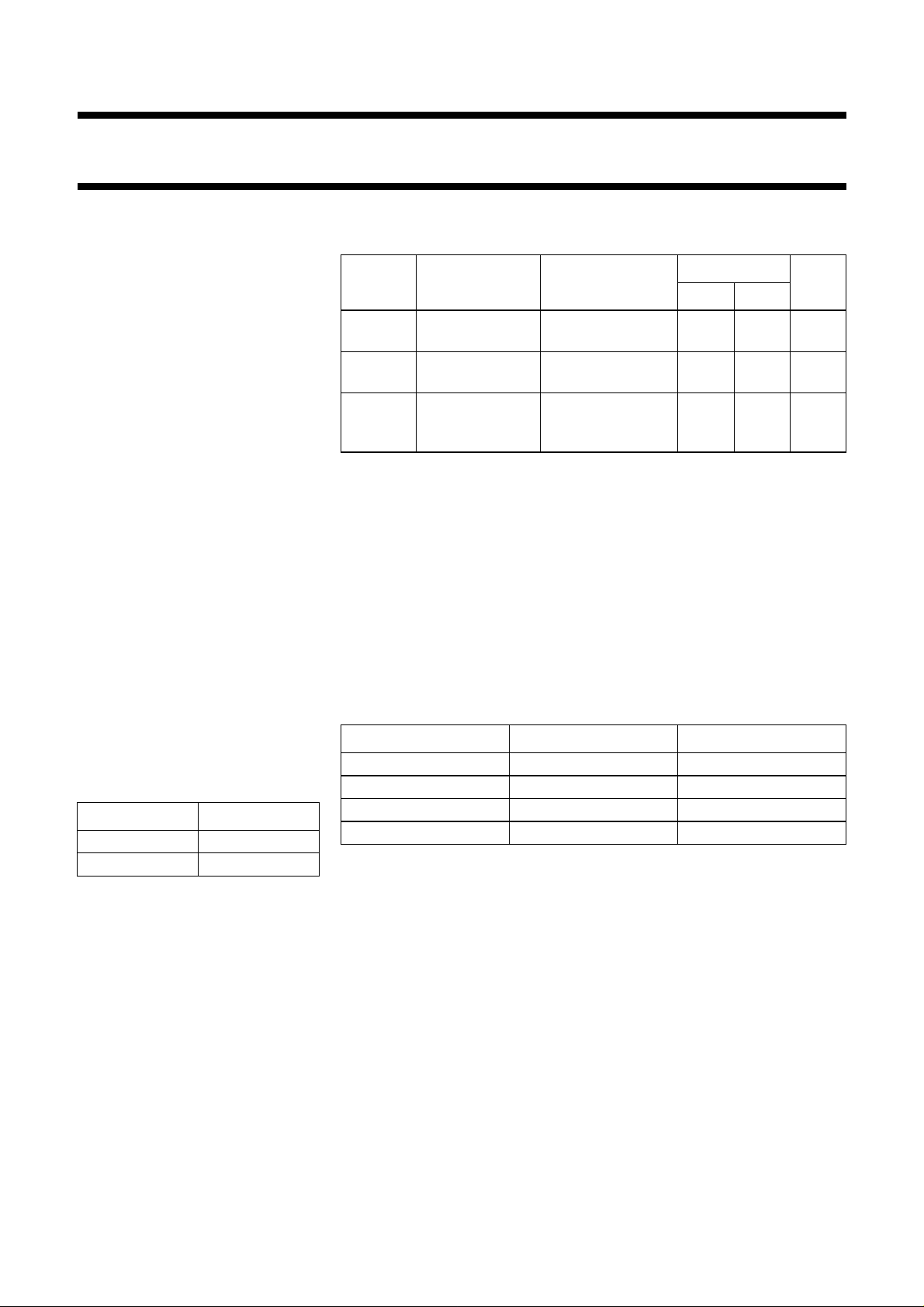
QUICK REFERENCE DATA
GND = 0 V; T
=25°C; tr=tf≤3.0 ns.
amb
SYMBOL PARAMETER CONDITIONS
t
PHL/tPLH
C
I
propagation
delay nA to nY
input
CL=15pF;
VCC=5V
VI=VCCor GND 4.0 4.0 pF
capacitance
C
PD
powerdissipation
capacitance
CL=50pF;
f = 1 MHz;
notes 1 and 2
Notes
1. C
is used to determine the dynamic power dissipation (PDin µW).
PD
PD=CPD× V
2
× fi+ ∑ (CL× V
CC
2
× fo) where:
CC
fi= input frequency in MHz;
fo= output frequency in MHz;
∑ (CL× V
2
× fo) = sum of outputs;
CC
CL= output load capacitance in pF;
VCC= supply voltage in Volts.
2. The condition is VI= GND to VCC.
TYPICAL
UNIT
AHC AHCT
3.0 3.0 ns
13.5 13.9 pF
The 74AHC/AHCT04 provide six
inverting buffers.
FUNCTION TABLE
See note 1.
INPUT nA OUTPUT nY
LH
HL
Note
1. H = HIGH voltage level;
L = LOW voltage level.
PINNING
PIN SYMBOL DESCRIPTION
1, 3, 5, 9, 11 and 13 1A to 6A data inputs
2, 4, 6, 8, 10 and 12 1Y to 6Y data outputs
7 GND ground (0 V)
14 V
CC
DC supply voltage
1999 Sep 27 2

Philips Semiconductors Product specification
Hex inverter 74AHC04; 74AHCT04
ORDERING INFORMATION
OUTSIDE NORTH
AMERICA
NORTH AMERICA
PINS PACKAGE MATERIAL CODE
PACKAGES
74AHC04D 74AHC04D 14 SO plastic SOT108-1
74AHC04PW 74AHC04PW DH 14 TSSOP plastic SOT402-1
74AHCT04D 74AHCT04D 14 SO plastic SOT108-1
74AHCT04PW 74AHCT04PW DH 14 TSSOP plastic SOT402-1
handbook, halfpage
1A
1Y
2A
2Y
3A
3Y
GND
1
2
3
4
04
5
6
7
MNA340
V
14
CC
13
6A
12
6Y
11
5A
10
5Y
9
4A
8
4Y
handbook, halfpage
A
Y
MNA341
handbook, halfpage
Fig.1 Pin configuration.
1Y
2Y
3Y
4Y
5Y
6Y
2
4
6
8
10
12
1A
1
2A
3
3A
5
4A
9
5A
11
6A
13
MNA342
Fig.3 Functional diagram.
handbook, halfpage
Fig.2 Logic diagram (one gate).
1
3
5
9
11
13
1
1
1
1
1
1
2
4
6
8
10
12
MNA343
Fig.4 IEC logic symbol.
1999 Sep 27 3

Philips Semiconductors Product specification
Hex inverter 74AHC04; 74AHCT04
RECOMMENDED OPERATING CONDITIONS
SYMBOL PARAMETER CONDITIONS
UNIT
MIN. TYP. MAX. MIN. TYP. MAX.
74AHC 74AHCT
V
CC
V
I
V
O
T
amb
DC supply voltage 2.0 5.0 5.5 4.5 5.0 5.5 V
input voltage 0 − 5.5 0 − 5.5 V
output voltage 0 − V
operating ambient temperature
range
see DC and AC
characteristics per
−40 +25 +85 −40 +25 +85 °C
−40 +25 +125 −40 +25 +125 °C
0 − V
CC
CC
V
device
t
(∆t/∆f) input rise and fall times except
r,tf
for Schmitt-trigger inputs
VCC= 3.3 V ±0.3 V −−100 −−−ns/V
=5V±0.5 V −−20 −−20
V
CC
LIMITING VALUES
In accordance with the Absolute Maximum Rating System (IEC 134); voltages are referenced to GND (ground= 0 V).
SYMBOL PARAMETER CONDITIONS MIN. MAX. UNIT
V
CC
V
I
I
IK
I
OK
I
O
I
CC
T
stg
P
D
DC supply voltage −0.5 +7.0 V
input voltage range −0.5 +7.0 V
DC input diode current VI< −0.5 V; note 1 −−20 mA
DC output diode current VO< −0.5 Vor VO>VCC+ 0.5 V; note 1 −±20 mA
DC output source or sink current −0.5V<VO<VCC+ 0.5 V −±25 mA
DC VCC or GND current −±75 mA
storage temperature range −65 +150 °C
power dissipation per package for temperature range: −40 to +125 °C; note 2 − 500 mW
Notes
1. The input and output voltage ratings may be exceeded if the input and output current ratings are observed.
2. For SO packages: above 70 °C the value of P
derates linearly with 8 mW/K.
D
For TSSOP packages: above 60 °C the value of PDderates linearly with 5.5 mW/K.
1999 Sep 27 4
Philips Semiconductors Product specification
Hex inverter 74AHC04; 74AHCT04
DC CHARACTERISTICS
74AHC family
Over recommended operating conditions; voltage are referenced to GND (ground = 0 V).
SYMBOL PARAMETER
V
IH
HIGH-level input
voltage
V
IL
LOW-level input
voltage
V
OH
HIGH-level output
voltage; all
outputs
HIGH-level output
voltage
V
OL
LOW-level output
voltage; all
outputs
LOW-level output
voltage
I
I
input leakage
current
I
OZ
3-state output
OFF current
I
CC
quiescent supply
current
C
I
input capacitance −−310−10 − 10 pF
TEST CONDITIONS T
25 −40 to +85 −40 to +125
amb
(°C)
UNIT
OTHER VCC(V)
MIN. TYP. MAX. MIN. MAX. MIN. MAX.
2.0 1.5 −−1.5 − 1.5 − V
3.0 2.1 −−2.1 − 2.1 −
5.5 3.85 −−3.85 − 3.85 −
2.0 −− 0.5 − 0.5 − 0.5 V
3.0 −− 0.9 − 0.9 − 0.9
5.5 −− 1.65 − 1.65 − 1.65
VI=VIHor VIL;
IO= −50 µA
2.0 1.9 2.0 − 1.9 − 1.9 − V
3.0 2.9 3.0 − 2.9 − 2.9 −
4.5 4.4 4.5 − 4.4 − 4.4 −
V
I=VIH
or VIL;
3.0 2.58 −−2.48 − 2.40 − V
IO= −4.0 mA
V
I=VIH
or VIL;
4.5 3.94 −−3.8 − 3.70 −
IO= −8.0 mA
VI=VIHor VIL;
IO=50µA
2.0 − 0 0.1 − 0.1 − 0.1 V
3.0 − 0 0.1 − 0.1 − 0.1
4.5 − 0 0.1 − 0.1 − 0.1
V
I=VIH
or VIL;
3.0 −− 0.36 − 0.44 − 0.55 V
IO=4mA
V
I=VIH
or VIL;
4.5 −− 0.36 − 0.44 − 0.55
IO=8mA
VI=VCCor GND 5.5 −− 0.1 − 1.0 − 2.0 µA
VI=VIHor VIL;
5.5 −− ±0.25 −±2.5 −±10.0 µA
VO=VCCor GND
VI=VCCor GND;
5.5 −− 4.0 − 40 − 80 µA
IO=0
1999 Sep 27 5
 Loading...